|
|
|
PDF SH67L17 Data sheet ( Hoja de datos )
| Número de pieza | SH67L17 | |
| Descripción | 24K 4-bit Microcontroller | |
| Fabricantes | Sino Wealth | |
| Logotipo | ||
Hay una vista previa y un enlace de descarga de SH67L17 (archivo pdf) en la parte inferior de esta página. Total 30 Páginas | ||
|
No Preview Available !
SH67L17
24K 4-bit Micro-controller with LCD Driver
Features
SH6610D-based single-chip 4-bit micro-controller with LCD
driver
ROM: 24K X 16bits
RAM: 4136 X 4 bits
- 43 System Control Register
- 4093 Data memory
- 180 LCD RAM
Operation Voltage: 1.2V - 1.7V (Typical 1.5V)
16 CMOS Bi-directional I/O Pins
8-Level Stack (Including Interrupts)
One 8-bit Base Timer
Warm-Up Timer
Powerful Interrupt Sources:
- External interrupt ( INT share with PORTA.0)
- Base timers interrupt
- PORTB & PORTC interrupts (Falling edge)
2 Clock Sources
OSC: (Code Option selects the type of OSC)
- Crystal Oscillator: 32.768kHz
- RC Oscillator:
131kHz
OSCX:
- RC oscillator:
500kHz (ROSCX)
Instruction Cycle Time (4/fOSC)
Two Low Power Operation Modes: HALT And STOP
Special HALT/STOP mode
Reset
- Built-in Watchdog Timer (WDT) (Code Option)
- Built-in Power-on Reset (POR)
- RESET 0 & RESET 1
LCD Driver:
- 60SEG X 9COM (1/9 Duty, 1/4 Bias)
Built-in Pull-high Resistor For PORTA - PORTD
Built-in Voltage Fourfold Charge Pump Circuit
8 X 8 BCD hardware multiplier
16/8 BCD hardware divider
RAM common space in every RAM bank
Low power consumption
Available in CHIP FORM
General Description
SH67L17 is a single-chip 4-bit micro-controller. This device integrates a SH6610D CPU core, RAM, ROM, Base Timer, a
hardware multiplier, a hardware divider, LCD driver, I/O ports, and voltage pump circuit. The SH67L17 is suitable for scientific
calculator application.
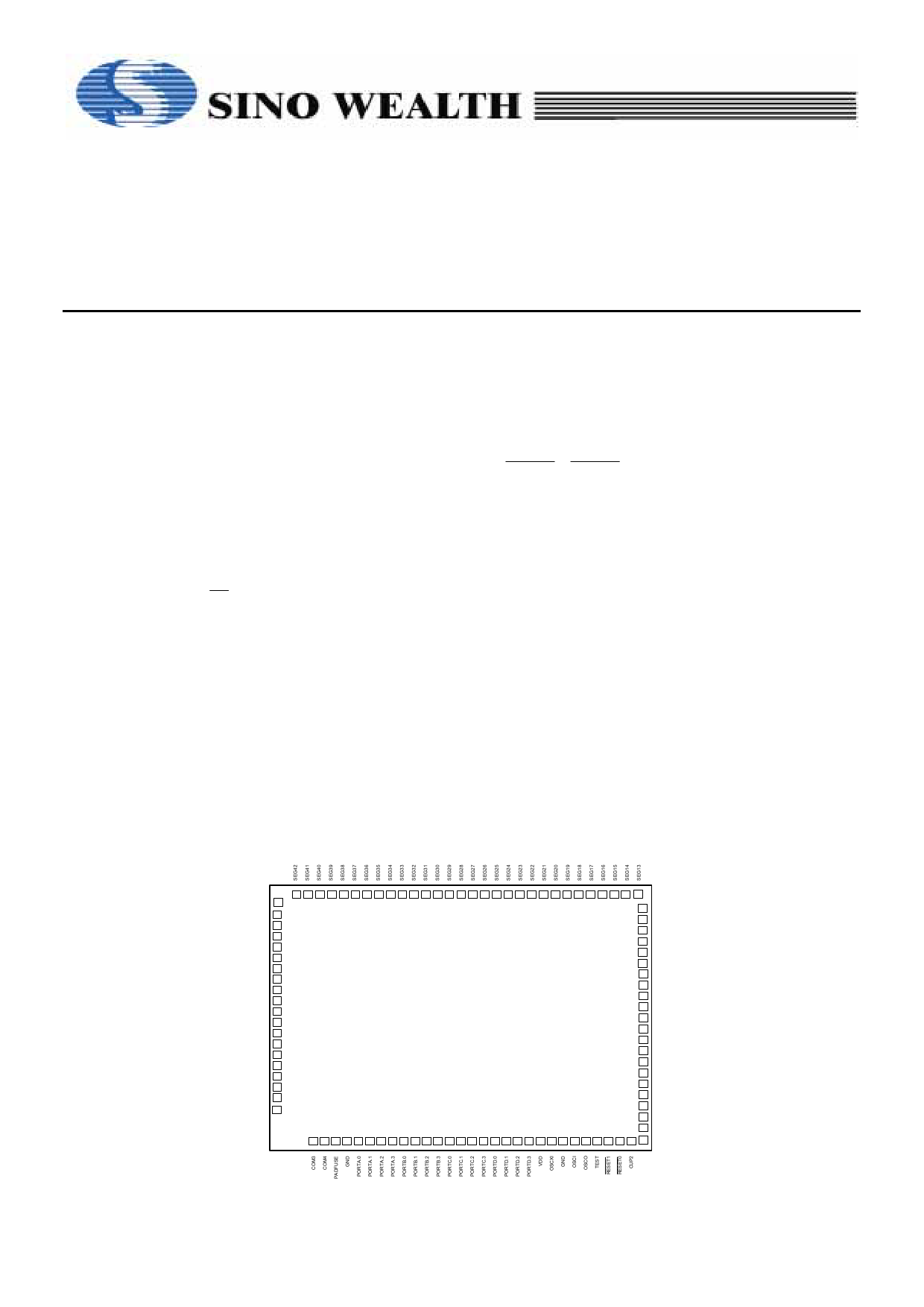
Pad Configuration
SEG43 82
SEG44
SEG45
83
84
SEG46 85
SEG47 86
SEG48 87
SEG49 88
SEG50 89
SEG51 90
SEG52 91
SEG53 92
SEG54 93
SEG55 94
SEG56 95
SEG57 96
SEG58 97
SEG59
SEG60
COM1
98
99
100
COM2 101
81 80 79 78 77 76 75 74 73 72 71 70 69 68 67 66 65 64 63 62 61 60 59 58 57 56 55 54 53 52
51 SEG12
50 SEG11
49 SEG10
48 SEG9
47 SEG8
46 SEG7
45 SEG6
44 SEG5
SH67L17
43 SEG4
42 SEG3
41 SEG2
40 SEG1
39 COM5
38 COM6
37 COM7
36 COM8
35 COM9
34 VP4
33 VP3
32 VP2
31 VP1
1 2 3 4 5 6 7 8 9 10 11 12 13 14 15 16 17 18 19 20 21 22 23 24 25 26 27 28 29 30 CUP1
1 V2.0
1 page 
SH67L17
RAM bank table: (RAMB: System Register $13 Bit2, 1, 0)
Bank0
Bank1
Bank2
Bank3
Bank4
Bank5
RAMB = 000 RAMB = 000 RAMB = 000 RAMB = 000 RAMB = 000 RAMB = 000
B=0
B=1
B=2
B=3
B=4
B=5
$060 - $07F $080 - $0FF $100 - $17F $180 - $1FF $200 - $27F $280 - $2FF
Bank8
RAMB = 001
B=0
$460 - $47F
Bank9
RAMB = 001
B=1
$480 - $4FF
Bank10
RAMB = 001
B=2
$500 - $57F
Bank11
RAMB = 001
B=3
$580 - $5FF
Bank12
RAMB = 001
B=4
$600 - $67F
Bank13
RAMB = 001
B=5
$680 - $6FF
Bank16
Bank17
Bank18
Bank19
Bank20
Bank21
RAMB = 010 RAMB = 010 RAMB = 010 RAMB = 010 RAMB = 010 RAMB = 010
B=0
B=1
B=2
B=3
B=4
B=5
$860 - $87F $880 - $8FF $900 - $97F $980 - $9FF $A00 - $A7F $A80 - $AFF
Bank24
Bank25
Bank26
Bank17
Bank28
Bank29
RAMB = 011 RAMB = 011 RAMB = 011 RAMB = 011 RAMB = 011 RAMB = 011
B=0
B=1
B=2
B=3
B=4
B=5
$C60 - $C7F $C80 - $CFF $D00 - $D7F $D80 - $DFF $E00 - $E7F $E80 - $EFF
Bank32
Bank33
Bank34
Bank35
Bank36
RAMB = 100 RAMB = 100 RAMB = 100 RAMB = 100 RAMB = 100
B=0
B=1
B=2
B=3
B=4
$1060 - $107F $1080 - $10FF $1100 - $117F $1180 - $11FF $1200 - $1267
Bank 6
RAMB = 000
B=6
$300 - $37F
Bank14
RAMB = 001
B=6
$700 - $77F
Bank22
RAMB = 010
B=6
$B00 - $B7F
Bank30
RAMB = 011
B=6
$F00 - $F7F
Bank7
RAMB = 000
B=7
$380 - $3FF
Bank15
RAMB = 001
B=7
$780 - $7FF
Bank23
RAMB = 010
B=7
$B80 - $BFF
Bank31
RAMB = 011
B=7
$F80 - $FFF
Where, B: RAM bank bit use in instructions
2.2. Configuration of System Register:
Address Bit 3
Bit 2
Bit 1
Bit 0 R/W
Remarks
$00 IEX
-
IEBT
IEP R/W Interrupt enable flags register
$01 IRQX
- IRQBT IRQP R/W Interrupt request flags register
$02 -
-
GO/DONE
M/D
R/W
Bit0: Multiplier/Divider mode control register
Bit1: Multiplier/Divider status flag register
$03
RST
BTM.2
BTM.1
BTM.0
R/W Bit2-0: Base timer mode register
R Bit3: RESET 0 / RESET 1 causes system reset control register
$04 MLTL.3 MLTL.2 MLTL.1 MLTL.0 R/W Multiplicator low nibble/Dividend low nibble register
$05 MLTH.3 MLTH.2 MLTH.1 MLTH.0 R/W Multiplicator high nibble/Dividend middle0 nibble register
$06 MLDL.3 MLDL.2 MLDL.1 MLDL.0 R/W Multiplicand low nibble/Dividend middle1 nibble register
$07 MLDH.3 MLDH.2 MLDH.1 MLDH.0 R/W Multiplicand high nibble/Dividend high nibble register
$08 PA.3 PA.2 PA.1 PA.0 R/W PORTA data register
$09 PB.3 PB.2 PB.1 PB.0 R/W PORTB data register
$0A PC.3 PC.2 PC.1 PC.0 R/W PORTC data register
$0B PD.3 PD.2 PD.1 PD.0 R/W PORTD data register
$0C DIVL.3 DIVL.2 DIVL.1 DIVL.0 R/W Divisor low nibble register
$0D DIVH.3 DIVH.2 DIVH.1 DIVH.0 R/W Divisor high nibble register
$0E TBR.3 TBR.2 TBR.1 TBR.0 R/W Table Branch Register
$0F
INX.3
INX.2
INX.1
INX.0 R/W Pseudo index register
5
5 Page 
SH67L17
5.5. Control of Oscillator
The oscillator control register configuration is shown as follows.
Address Bit 3
Bit 2
$1D SPDUP
-
X-
X-
Bit 1
OXM
X
X
Bit 0
OXON
0
1
R/W Remarks
Bit0: OSCX oscillation on/off control register
R/W
Bit1: system clock select register
Bit3: Speed up the 32.768kHz Crystal Oscillator in the CPU
turn-on status control register
Turn off OSCX oscillation
Turn on OSCX oscillation
X - 0X
Select OSC as system clock
X - 1X
0 - XX
Select OSCX as system clock
Turn off the Speed-up function
1 - XX
Turn on the Speed-up function
It is recommended to turn off the” Speed up the 32.768kHz Crystal Oscillator in the CPU turn-on status” function when
32.768kHz Crystal is stable.
When OXON is clear to “0”, OXM will be clear to “0” by hardware.
Programming Notes:
It takes at least 5ms for the OSCX oscillation circuit to go on until the oscillation stabilizes. When the CPU system clock switching
from OSC to OSCX, the user has to wait at least 5ms till the OSCX oscillation is activated. In addition, the start time varies a lot
with respect to oscillator characteristics and operational conditions. Therefore the waiting time depends on applications. When
switching from OSCX to OSC, and turning off OSCX in one instruction, the OSCX turns off control would be delayed for one
instruction cycle automatically to prevent CPU operation error.
5.6. Capacitor Selection for Oscillator
*- The specified ceramic resonator has internal built-in load capacity
Crystal Oscillator
Frequency
C1
C2
Recommend Type
Manufacturer
32.768kHz 5 - 12.5pF 5 - 12.5pF
DT 38 (φ3x8)
φ3x8 - 32.768KHz
KDS
Vectron International
Notes:
1. Capacitor values are used for design guidance only!
2. These capacitors were tested with the crystals listed above for basic start-up and operation. They are not optimized.
3. Be careful for the stray capacitance on PCB board, the user should test the performance of the oscillator over the expected
VDD and the temperature range for the application.
Before selecting crystal/ceramic, the user should consult the crystal/ceramic manufacturer for appropriate value of external
component to get best performance, visit http://www.sinowealth.com for more recommended manufactures
11
11 Page | ||
| Páginas | Total 30 Páginas | |
| PDF Descargar | [ Datasheet SH67L17.PDF ] | |
Hoja de datos destacado
| Número de pieza | Descripción | Fabricantes |
| SH67L17 | 24K 4-bit Microcontroller | Sino Wealth |
| SH67L17A | 24K 4-bit Microcontroller | Sino Wealth |
| SH67L18 | 8K 4-bit Low Power Micro-controller | Sino Wealth Microelectronic |
| SH67L19 | 4K 4-Bit Micro Controller | Sino Wealth Microelectronic |
| Número de pieza | Descripción | Fabricantes |
| SLA6805M | High Voltage 3 phase Motor Driver IC. |
Sanken |
| SDC1742 | 12- and 14-Bit Hybrid Synchro / Resolver-to-Digital Converters. |
Analog Devices |
|
DataSheet.es es una pagina web que funciona como un repositorio de manuales o hoja de datos de muchos de los productos más populares, |
| DataSheet.es | 2020 | Privacy Policy | Contacto | Buscar |