|
|
|
PDF AP3776B Data sheet ( Hoja de datos )
| Número de pieza | AP3776B | |
| Descripción | LOW POWER OFF-LINE PRIMARY SIDE REGULATION CONTROLLER | |
| Fabricantes | Diodes | |
| Logotipo | ||
Hay una vista previa y un enlace de descarga de AP3776B (archivo pdf) en la parte inferior de esta página. Total 17 Páginas | ||
|
No Preview Available !
AP3776B
LOW POWER OFF-LINE PRIMARY SIDE REGULATION CONTROLLER
Description
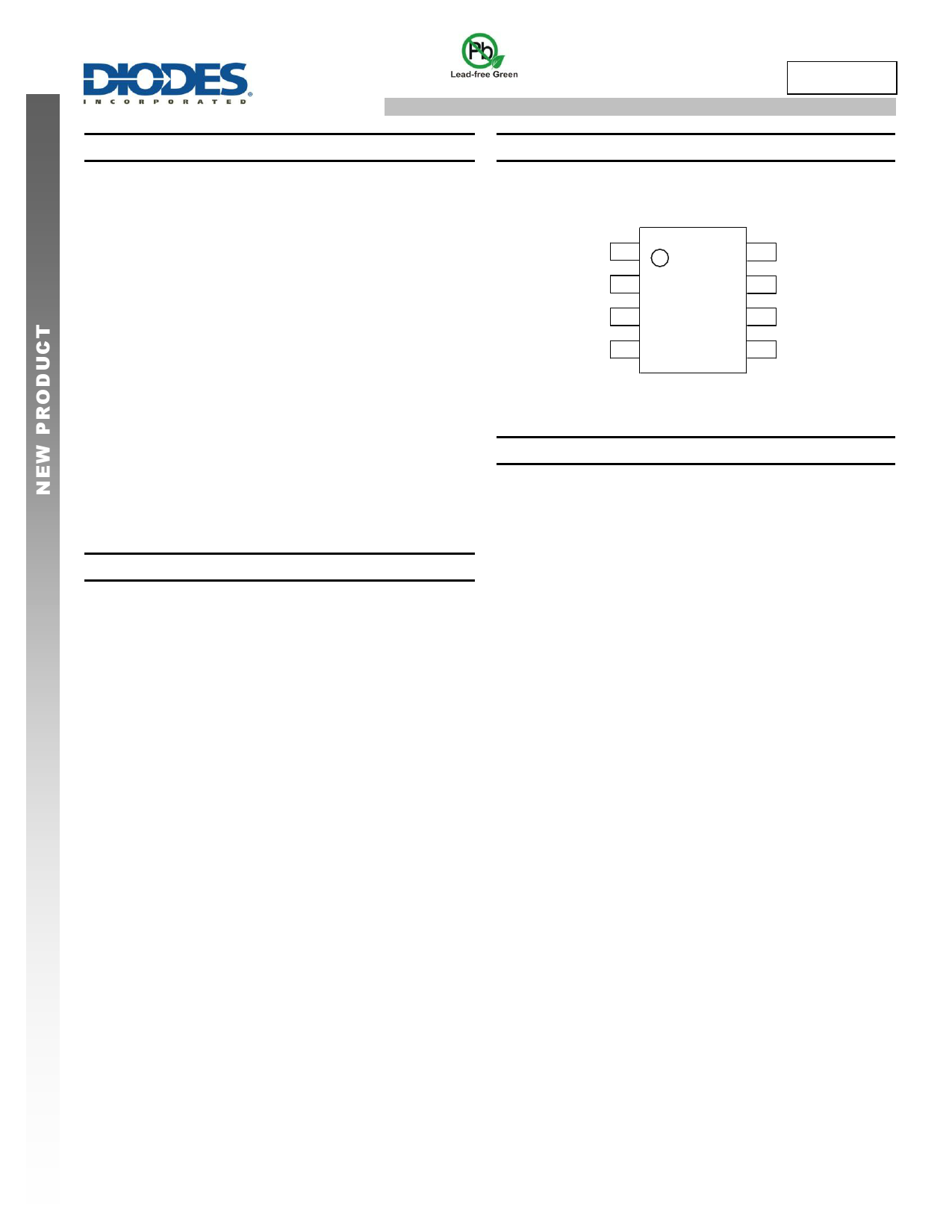
Pin Assignments
The AP3776B is a high performance AC/DC power supply controller
for battery charger and adapter applications. It can meet less than
10mW standby power for “Super Star” charger criteria. The device
uses Pulse Frequency Modulation (PFM) method to build
discontinuous conduction mode (DCM) flyback power supplies.
The AP3776B provides accurate constant voltage (CV), constant
current (CC) and outstanding dynamic performance without requiring
an opto-coupler. It also eliminates the need of loop compensation
circuitry while maintaining stability.
(Top View)
IS 1
EM 2
VCC 3
OUT 4
8 FB
7 CPC
6 VCS
5 GND
The AP3776B achieves excellent regulation and high average
efficiency, less than 10mW no-load power consumption and less than
1s startup time. When AP3776B is used with AP4341, APR343 or
APR3415, good under-shoot performance and higher conversion
efficiency can be achieved.
The AP3776B is available in SO-8 package.
SO-8
Applications
Adapter/Chargers for Shaver, Cell/Cordless Phones, PDAs, MP3
and Other Portable Apparatus
Standby and Auxiliary Power Supplies
Features
Primary Side Control for Eliminating Opto-coupler
10mW No-load Input Power
Compensation for External Component Temperature Variations
Flyback Topology in DCM Operation
Random Frequency Adjustment to Reduce System EMI
Semi-valley Turn on for the Higher Efficiency
Built-in Soft Start
Over Voltage Protection
Over Temperature Protection
Short Circuit Protection
AP4341, APR343 or APR3415 Awaking Signal Detection
Audio Noise Reduction
Internal Cable Compensation
SO-8 Package
Totally Lead-Free & Fully RoHS Compliant (Notes 1 & 2)
Halogen and Antimony Free. “Green” Device (Note 3)
Notes:
1. No purposely added lead. Fully EU Directive 2002/95/EC (RoHS) & 2011/65/EU (RoHS 2) compliant.
2. See http://www.diodes.com/quality/lead_free.html for more information about Diodes Incorporated’s definitions of Halogen- and Antimony-free, "Green"
and Lead-free.
3. Halogen- and Antimony-free "Green” products are defined as those which contain <900ppm bromine, <900ppm chlorine (<1500ppm total Br + Cl) and
<1000ppm antimony compounds.
AP3776B
Document number: DS36737 Rev. 6 - 2
1 of 17
www.diodes.com
December 2015
© Diodes Incorporated
1 page 
AP3776B
Absolute Maximum Ratings (Note 4)
Symbol
Parameter
Rating
Unit
VCC Voltage at VCC to GND
– Voltage at OUT, EM to GND
-0.3 to 28
-0.3 to 23
V
V
– Voltage at IS, VCS, CPC to GND
– FB Input
– Output Current at OUT
-0.3 to 7
-40 to 10
Internally limited
V
V
A
TJ Operating Junction Temperature
+150
ºC
TSTG
Storage Temperature
-65 to +150
ºC
TLEAD
θJA
ESD
Lead Temperature (Soldering, 10 Sec)
Thermal Resistance Junction-to-Ambient
Electrostatic Discharge
Capability
Human Body Model
Charged Device Model
Machine Model
+300
190
6000
2500
200
ºC
ºC/W
V
V
V
Note 4: Stresses greater than those listed under “Absolute Maximum Ratings” may cause permanent damage to the device. These are stress ratings only, and
functional operation of the device at these or any other conditions beyond those indicated under “Recommended Operating Conditions” is not implied.
Exposure to “Absolute Maximum Ratings” for extended periods may affect device reliability.
Electrical Characteristics (@TA = +25°C, VCC = 15V, unless otherwise specified.)
Symbol
Parameter
UVLO SECTION
VTH(ST)
Start-up Threshold
VOPR(Min)
Minimal Operating Voltage
STANDBY CURRENT SECTION
IST Start-up Current
ICC(STB)
Standby Mode Quiescent Current
ICC(QST)
Normal Mode Quiescent Current
CURRENT SENSE SECTION
VCS Current Sense Threshold (Note 5)
tLEB Leading Edge Blanking (Note 6)
FEEDBACK INPUT SECTION
RFB Input Resistance of FB Pin
VFB Feedback Threshold Voltage
LINE COMPENSATION SECTION
Line Compensation Transconductance
gm (Note 7)
Conditions
–
After turning on
VCC = VTH(ST)-1V,
Before turning on
No load at OUT pin,
Standby Mode
No load at OUT pin,
Normal Mode
–
–
VFB = 4V
–
–
Min Typ Max Unit
11 13 14
5.3 6.1 7.0
V
0 0.2 0.6
60 100 130
160 280 330
µA
425 450 465 mV
300 500 700
ns
0.5 0.7 0.9 MΩ
3.64 3.7 3.76
V
0.55 0.7 0.85 µS
AP3776B
Document number: DS36737 Rev. 6 - 2
5 of 17
www.diodes.com
December 2015
© Diodes Incorporated
5 Page 
Function Description (Cont.)
VCSREF
VCS_H
VCS_M
High-load
Medium-load
VCS_L
LL mode Light-load
fsw
60kHz
24kHz
Iomax
AP3776B
Iomax
Figure 4. Multiple Segment Peak Current at CV Mode
3. The LL Mode Operating (Typical Application with APR343)
At no load and light load, the AP3776B works in Low Light mode (LL mode) and the output voltage is detected by APR343. In order to achieve
ultra low standby power in LL mode, the static current (ICC_NL) of the AP3776B is reduced from 280μA to 100μA.
• The conditions of exiting LL mode---VCPC>65mV or tOFF<tDELAY+30μs
• The conditions of entering LL mode---VCPC<33mV and tOFF≥tDELAY+30μs
In LL mode, when the APR343 detects the output voltage is lower than its trigger voltage, the APR343 VDET pin emits a periodical pulse
current. This pulse current will generate a pulse voltage on feedback winding through the transformer coupling. When the AP3776B detects this
VPULSE (>100mV is valid), primary switch immediately turns on to provide one energy pulse to supply output terminal and primary VCC. To
achieve low standby power, the lower switching frequency is necessary. But if the off time is too long, the VCC voltage will reduce to very low
level. To avoid VCC being lower than VOPR(Min), a minimum switching frequency is specified by the APR343 (tDIS). If VOUT does not fall below
trigger voltage during tDIS, APR343 VDET pin will emit the periodical pulse current and let the primary switch turn on.
4. Leading Edge Blanking
When the power switch is turned on, a turn-on spike will occur on the sense-resistor. To avoid false-termination of the switching pulse, a 500ns
leading-edge blanking (from power MOSFET on) is built in. During this blanking period, the current sense comparator is disabled and the gate
driver can’t be switched off.
5. Adjustable Line Compensation
Since there is a constant delay time from the CS pin voltage reaching the given VCS reference to the power MOSFET turning off, the real
primary peak current value always has a gap with the ideal value. The gap value changes with different input line voltage, which is caused by
different current rising slope, results in different system constant current value.
In order to eliminate the constant current deviation due to line voltage, the adjustable line compensation is introduced to AP3776B design. By
sensing the negative voltage of FB pin which is linear to the line voltage, a current (ILINE) proportional to line voltage flows out from the CS pin to
the resistor RLINE, and create an adjustable compensation voltage to clear up the primary current gap, so that the excellent line regulation of
output current will be achieved.
VCS _ LINE
RLINE
0.4 1
700k
RFB 2
RFB1 RFB 2
N aux
Np
Vin d c
AP3776B
Document number: DS36737 Rev. 6 - 2
11 of 17
www.diodes.com
December 2015
© Diodes Incorporated
11 Page | ||
| Páginas | Total 17 Páginas | |
| PDF Descargar | [ Datasheet AP3776B.PDF ] | |
Hoja de datos destacado
| Número de pieza | Descripción | Fabricantes |
| AP3776 | LOW POWER OFF-LINE PRIMARY SIDE REGULATION CONTROLLER | Diodes |
| AP3776B | LOW POWER OFF-LINE PRIMARY SIDE REGULATION CONTROLLER | Diodes |
| Número de pieza | Descripción | Fabricantes |
| SLA6805M | High Voltage 3 phase Motor Driver IC. |
Sanken |
| SDC1742 | 12- and 14-Bit Hybrid Synchro / Resolver-to-Digital Converters. |
Analog Devices |
|
DataSheet.es es una pagina web que funciona como un repositorio de manuales o hoja de datos de muchos de los productos más populares, |
| DataSheet.es | 2020 | Privacy Policy | Contacto | Buscar |