|
|
|
PDF IDT8N0Q001 Data sheet ( Hoja de datos )
| Número de pieza | IDT8N0Q001 | |
| Descripción | Quad-Frequency Programmable XO | |
| Fabricantes | IDT | |
| Logotipo | ||
Hay una vista previa y un enlace de descarga de IDT8N0Q001 (archivo pdf) en la parte inferior de esta página. Total 17 Páginas | ||
|
No Preview Available !
Quad-Frequency Programmable XO IDT8N0Q001 REV H
DATASHEET
General Description
The IDT8N0Q001 is a Quad-Frequency Programmable Clock
Oscillator with very flexible frequency programming capabilities. The
device uses IDT’s fourth generation FemtoClock® NG technology for
an optimum of high clock frequency and low phase noise
performance. The device accepts 2.5V or 3.3V supply and is
packaged in a small, lead-free (RoHS 6) 10-lead ceramic 5mm x
7mm x 1.55mm package.
Besides the 4 default power-up frequencies set by the FSEL0 and
FSEL1 pins, the IDT8N0Q001 can be programmed via the I2C
interface to output clock frequencies between 15.476 to 260MHz to a
very high degree of precision with a frequency step size of
435.9Hz ÷ N (N: PLL post divider). Since the FSEL0 and FSEL1 pins
are mapped to 4 independent PLL M and N divider registers (P, MINT,
MFRAC and N), reprogramming those registers to other frequencies
under control of FSEL0 and FSEL1 is supported. The extended
temperature range supports wireless infrastructure,
telecommunication and networking end equipment requirements.
Features
• Fourth generation FemtoClock® NG technology
• Programmable clock output frequency from
15.476MHz to 260MHz
• Four power-up default frequencies (see part number order codes),
re-programmable by I2C
• I2C programming interface for the output clock frequency and
internal PLL control registers
• Frequency programming resolution is 435.9Hz ÷ N
• One 2.5V, 3.3V LVCMOS clock output
• Two control inputs for the power-up default frequency
• LVCMOS/LVTTL compatible control inputs
• RMS phase jitter @ 156.25MHz (12kHz - 20MHz):
0.250ps (typical)
• RMS phase jitter @ 156.25MHz (1kHz - 40MHz):
0.290ps (typical)
• 2.5V or 3.3V supply
• -40°C to 85°C ambient operating temperature
• Available in Lead-free (RoHS 6) package
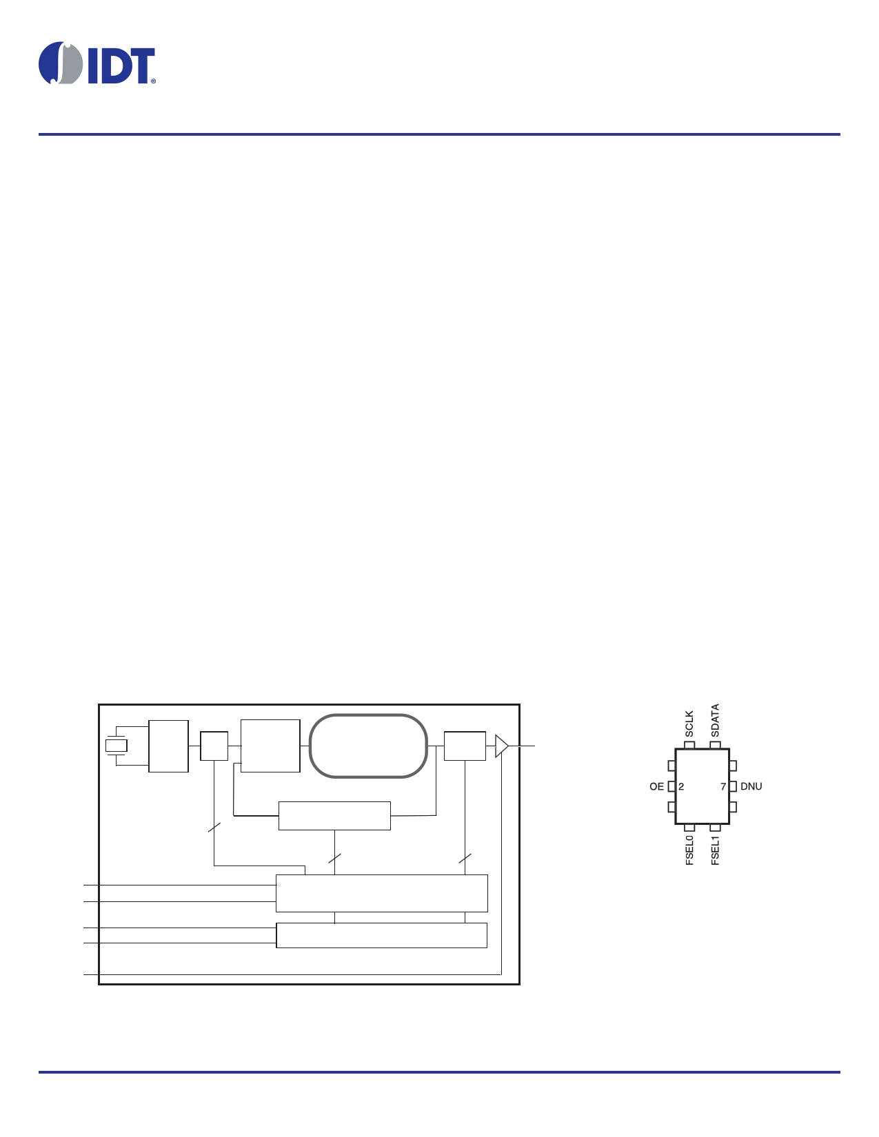
Block Diagram
OSC ÷P
fXTAL
2
FSEL1
FSEL0
SCLK
SDATA
OE
Pulldown
Pulldown
Pullup
Pullup
Pullup
PFD
&
LPF
FemtoClock® NG
VCO
1950-2600MHz
÷N
÷MINT, MFRAC
25
Configuration Register (ROM)
(Frequency, APR, Polarity)
7
I2C Control
Pin Assignment
Q
10 9
DNU 1
8 VDD
GND 3
6Q
45
IDT8N0Q001 Rev H
10-lead ceramic 5mm x 7mm x 1.55mm
package body
CD Package
Top View
IDT8N0Q001HCD REVISION A APRIL 4, 2014
1
©2014 Integrated Device Technology, Inc.
1 page 
IDT8N0Q001REV H Data Sheet
QUAD-FREQUENCY PROGRAMMABLE-XO
Absolute Maximum Ratings
NOTE: Stresses beyond those listed under Absolute Maximum Ratings may cause permanent damage to the device. These ratings are stress
specifications only. Functional operation of the product at these conditions or any conditions beyond those listed in the DC Characteristics or
AC Characteristics is not implied. Exposure to absolute maximum rating conditions for extended periods may affect product reliability.
Item
Supply Voltage, VDD
Inputs, VI
Outputs, VO (LVCMOS)
Outputs, IO (SDATA)
Package Thermal Impedance, JA
Storage Temperature, TSTG
Rating
3.6V
-0.5V to VDD + 0.5V
-0.5V to VDD + 0.5V
10mA
49.4°C/W (mps)
-65C to 150C
DC Electrical Characteristics
Table 5A. Power Supply DC Characteristics, VDD = 3.3V ± 5%, TA = -40°C to 85°C
Symbol
Parameter
Test Conditions
Minimum
VDD Positive Supply Voltage
IDD Power Supply Current
No Load, OE = Low
3.135
Typical
3.3
127
Maximum
3.465
145
Units
V
mA
Table 5B. Power Supply DC Characteristics, VDD = 2.5V ± 5%, TA = -40°C to 85°C
Symbol
Parameter
Test Conditions
Minimum
VDD Positive Supply Voltage
IDD Power Supply Current
No Load, OE = Low
2.375
Typical
2.5
123
Maximum
2.625
140
Units
V
mA
IDT8N0Q001HCD REVISION A APRIL 4, 2014
5
©2014 Integrated Device Technology, Inc.
5 Page 
IDT8N0Q001REV H Data Sheet
Parameter Measurement Information, continued
VOH
VREF
1σ contains 68.26% of all measurements
2σ contains 95.4% of all measurements
3σ contains 99.73% of all measurements
4σ contains 99.99366% of all measurements
6σ contains (100-1.973x10⁻⁷)% of all measurements
Reference Point
(Trigger Edge)
Histogram
Mean Period
(First edge after trigger)
VOL
Period Jitter
QUAD-FREQUENCY PROGRAMMABLE-XO
Applications Information
Recommendations for Unused Input Pins
Inputs:
LVCMOS Select Pins
All control pins have internal pulldowns and pullups; additional
resistance is not required but can be added for additional protection.
A 1k resistor can be used.
IDT8N0Q001HCD REVISION A APRIL 4, 2014
11
©2014 Integrated Device Technology, Inc.
11 Page | ||
| Páginas | Total 17 Páginas | |
| PDF Descargar | [ Datasheet IDT8N0Q001.PDF ] | |
Hoja de datos destacado
| Número de pieza | Descripción | Fabricantes |
| IDT8N0Q001 | Quad-Frequency Programmable XO | IDT |
| Número de pieza | Descripción | Fabricantes |
| SLA6805M | High Voltage 3 phase Motor Driver IC. |
Sanken |
| SDC1742 | 12- and 14-Bit Hybrid Synchro / Resolver-to-Digital Converters. |
Analog Devices |
|
DataSheet.es es una pagina web que funciona como un repositorio de manuales o hoja de datos de muchos de los productos más populares, |
| DataSheet.es | 2020 | Privacy Policy | Contacto | Buscar |