|
|
|
PDF MC74HCT259A Data sheet ( Hoja de datos )
| Número de pieza | MC74HCT259A | |
| Descripción | 8-Bit Addressable Latch 1-of-8 Decoder | |
| Fabricantes | ON Semiconductor | |
| Logotipo | ||
Hay una vista previa y un enlace de descarga de MC74HCT259A (archivo pdf) en la parte inferior de esta página. Total 9 Páginas | ||
|
No Preview Available !
MC74HCT259A
8-Bit Addressable Latch
1-of-8 Decoder with LSTTL
Inputs
High−Performance Silicon−Gate CMOS
The MC74HCT259A is identical in pinout to the LS259. The device
inputs are compatible with standard CMOS and LSTTL outputs.
The HCT259A has four modes of operation as shown in the mode
selection table. In the addressable latch mode, the data on Data In is
written into the addressed latch. The addressed latch follows the data
input with all non−addressed latches remaining in their previous
states. In the memory mode, all latches remain in their previous state
and are unaffected by the Data or Address inputs. In the one−of−eight
decoding or demultiplexing mode, the addressed output follows the
state of Data In with all other outputs in the LOW state. In the Reset
mode all outputs are LOW and unaffected by the address and data
inputs. When operating the HCT259A as an addressable latch,
changing more than one bit of the address could impose a transient
wrong address. Therefore, this should only be done while in the
memory mode.
Features
• Output Drive Capability: 10 LSTTL Loads
• Outputs Directly Interface to CMOS, NMOS, and TTL
• Operating Voltage Range: 4.5 to 5.5 V
• Low Input Current: 1 mA
• High Noise Immunity Characteristic of CMOS Devices
• These are Pb−Free Devices
http://onsemi.com
16
1
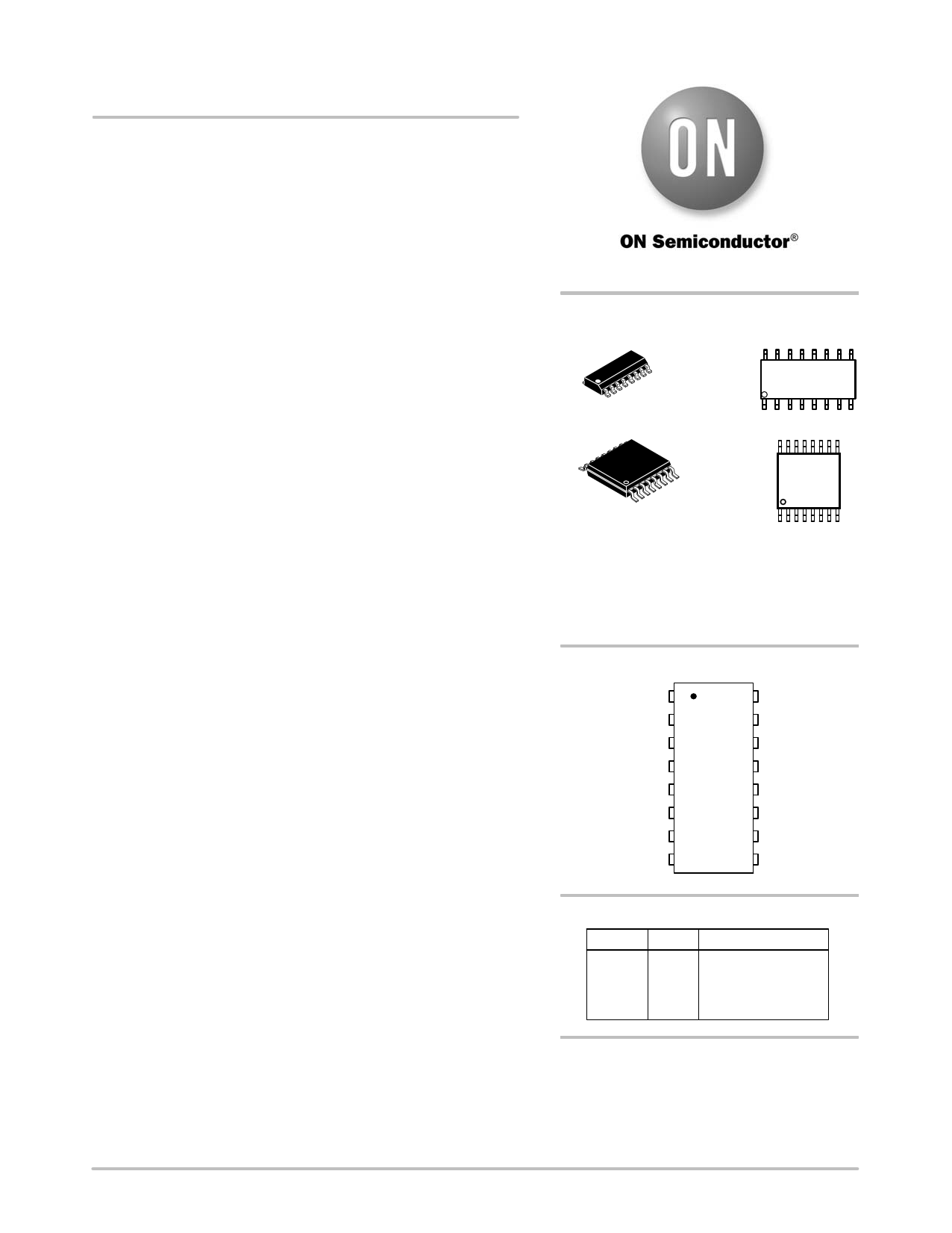
SOIC−16
D SUFFIX
CASE 751B
MARKING
DIAGRAMS
16
HCT259AG
AWLYWW
1
16
16
1
TSSOP−16
DT SUFFIX
CASE 948F
HCT
259A
ALYWG
G
1
A
WL, L
YY, Y
= Assembly Location
= Wafer Lot
= Year
WW, W = Work Week
G or G = Pb−Free Package
(Note: Microdot may be in either location)
PIN ASSIGNMENT
A0 1
A1 2
A2 3
Q0 4
Q1 5
Q2 6
Q3 7
GND 8
16 VCC
15 RESET
14 ENABLE
13 DATA IN
12 Q7
11 Q6
10 Q5
9 Q4
MODE SELECTION TABLE
Enable
L
H
L
H
Reset
H
H
L
L
Mode
Addressable Latch
Memory
8−Line Demultiplexer
Reset
ORDERING INFORMATION
See detailed ordering and shipping information in the package
dimensions section on page 6 of this data sheet.
© Semiconductor Components Industries, LLC, 2011
April, 2011 − Rev. 3
1
Publication Order Number:
MC74HCT259A/D
1 page 
MC74HCT259A
SWITCHING WAVEFORMS
DATA IN
tr
DATA IN
tPLH
OUTPUT Q
90%
1.3 V
10%
90%
1.3 V
10%
50%
tTLH
Figure 2.
tf
3.0 V
GND
tPHL
tTHL
ADDRESS
SELECT
OUTPUT Q
1.3 V
1.3 V
tPHL
50%
tPLH
Figure 3.
3.0V
GND
3.0V
GND
3.0V
GND
DATA IN
ENABLE
OUTPUT Q
tw
1.3 V
tPHL
3.0 V
tw
1.3 V 1.3 V
tPLH
GND
VCC
GND
50%
DATA IN
RESET
OUTPUT Q
Figure 4.
tw
1.3 V
tPHL
50%
Figure 5.
3.0V
GND
3.0V
GND
DATA IN
OR
ADDRESS
SELECT
1.3 V
ENABLE
th(H)
tsu
1.3 V
Figure 6.
TEST POINT
3.0V
GND
th(L)
tsu 3.0V
DEVICE
UNDER
TEST
OUTPUT
CL*
GND
*Includes all probe and jig capacitance
Figure 7. Test Circuit
http://onsemi.com
5
5 Page | ||
| Páginas | Total 9 Páginas | |
| PDF Descargar | [ Datasheet MC74HCT259A.PDF ] | |
Hoja de datos destacado
| Número de pieza | Descripción | Fabricantes |
| MC74HCT259A | 8-Bit Addressable Latch 1-of-8 Decoder | ON Semiconductor |
| Número de pieza | Descripción | Fabricantes |
| SLA6805M | High Voltage 3 phase Motor Driver IC. |
Sanken |
| SDC1742 | 12- and 14-Bit Hybrid Synchro / Resolver-to-Digital Converters. |
Analog Devices |
|
DataSheet.es es una pagina web que funciona como un repositorio de manuales o hoja de datos de muchos de los productos más populares, |
| DataSheet.es | 2020 | Privacy Policy | Contacto | Buscar |