|
|
PDF AD5593R Data sheet ( Hoja de datos )
| Número de pieza | AD5593R | |
| Descripción | Configurable ADC/DAC | |
| Fabricantes | Analog Devices | |
| Logotipo |  |
|
Hay una vista previa y un enlace de descarga de AD5593R (archivo pdf) en la parte inferior de esta página. Total 28 Páginas | ||
|
No Preview Available !
Data Sheet
8-Channel, 12-Bit, Configurable ADC/DAC
with On-Chip Reference, I2C Interface
AD5593R
FEATURES
8-channel, configurable ADC/DAC/GPIO
Configurable as any combination of
8 12-bit DAC channels
8 12-bit ADC channels
8 general-purpose I/O pins
Integrated temperature sensor
16-lead TSSOP package
I2C interface
APPLICATIONS
Control and monitoring
General-purpose analog and digital I/O
GENERAL DESCRIPTION
The AD5593R has eight input/output (I/O) pins, which can be
independently configured as digital-to-analog converter (DAC)
outputs, analog-to-digital converter (ADC) inputs, digital outputs,
or digital inputs. When an I/O pin is configured as an analog
output, it is driven by a 12-bit DAC. The output range of the
DAC is 0 V to VREF or 0 V to 2 × VREF. When an I/O pin is
configured as an analog input, it is connected to a 12-bit ADC
via an analog multiplexer. The input range of the ADC is 0 V to
VREF or 0 V to 2 × VREF. The I/O pins can also be configured to
be general-purpose, digital input or output (GPIO) pins. The
state of the GPIO pins can be set or read back by accessing the
GPIO write data register and GPIO read configuration registers,
respectively, via an I2C write or read operation.
The AD5593R has an integrated 2.5 V, 20 ppm/°C reference that
is turned off by default and an integrated temperature indicator
that gives an indication of the die temperature. The temperature
value is read back as part of an ADC read sequence.
The AD5593R is available in a 16-lead TSSOP and operates over
a temperature range of −40°C to +105°C.
Table 1. Related Products
Product
Description
AD5592R AD5593R equivalent with SPI interface
AD5592R-1 AD5593R equivalent with SPI interface and VLOGIC pin
FUNCTIONAL BLOCK DIAGRAM
VLOGIC
VDD
VREF
SCL
SDA
A0
RESET
AD5593R
POWER-ON
RESET
INPUT
REGISTER
DAC
REGISTER
DAC 0
2.5V
REFERENCE
GPIO0
I2C
INTERFACE
LOGIC
INPUT
REGISTER
DAC
REGISTER
DAC 7
SEQUENCER
TEMPERATURE
INDICATOR
12-BIT
SUCCESSIVE
APPROXIMATION
ADC
T/H
GPIO7
MUX
I/O0
I/O7
GND
Figure 1.
Rev. 0
Document Feedback
Information furnished by Analog Devices is believed to be accurate and reliable. However, no
responsibilityisassumedbyAnalogDevices for itsuse,nor foranyinfringementsofpatentsor other
rights of third parties that may result from its use. Specifications subject to change without notice. No
license is granted by implication or otherwise under any patent or patent rights of Analog Devices.
Trademarksandregisteredtrademarksarethepropertyoftheirrespectiveowners.
One Technology Way, P.O. Box 9106, Norwood, MA 02062-9106, U.S.A.
Tel: 781.329.4700
©2014 Analog Devices, Inc. All rights reserved.
Technical Support
www.analog.com
1 page 
Data Sheet
AD5593R
Parameter
LOGIC INPUTS
Input Voltage
High, VINH
Low, VINL
Input Current, IIN
Input Capacitance, CIN
LOGIC OUTPUT (SDA)
Output High Voltage, VOH
Output Low Voltage, VOL
Floating-State Output Capacitance
TEMPERATURE SENSOR2
Resolution
Operating Range
Accuracy
Track Time
POWER REQUIREMENTS
VDD
IDD
Power-Down Mode
Normal Mode
VDD = 5 V
VDD = 3 V
Min
Typ Max
Unit Test Conditions/Comments
0.7 × VLOGIC
−1 +0.01
0.3 × VLOGIC
+1
10
V
V
µA
pF
VLOGIC − 0.2
10
0.4
V
V
pF
12 Bits
−40
+105
°C
±3 °C
5 µs
20 µs
2.7 5.5 V
2.7
3.5 µA
1.6 mA
1 mA
2.4 mA
1.1 mA
1 mA
0.75 mA
0.5 mA
0.5 mA
1.1 mA
1 mA
1.1 mA
0.78 mA
0.75 mA
0.5 mA
0.45 mA
0.45 mA
ISOURCE = 200 µA; VDD = 2.7 V to 5.5 V
ISINK = 200 µA
ADC buffer enabled
ADC buffer disabled
Digital inputs = 0 V or VDD
I/O0 to I/O7 are DACs, internal reference, gain = 2
I/O0 to I/O7 are DACs, external reference, gain = 2
I/O0 to I/O7 are DACs and sampled by the ADC,
internal reference, gain = 2
I/O0 to I/O7 are DACs and sampled by the ADC,
external reference, gain = 2
I/O0 to I/O7 are ADCs, internal reference, gain = 2
I/O0 to I/O7 are ADCs, external reference, gain = 2
I/O0 to I/O7 are general-purpose outputs
I/O0 to I/O7 are general-purpose inputs
I/O0 to I/O7 are DACs, internal reference, gain = 1
I/O0 to I/O7 are DACs, external reference, gain = 1
I/O0 to I/O7 are DACs and sampled by the ADC,
internal reference, gain = 1
I/O0 to I/O7 are DACs and sampled by the ADC,
external reference, gain = 1
I/O0 to I/O7 are ADCs, internal reference, gain = 1
I/O0 to I/O7 are ADCs, external reference, gain = 1
I/O0 to I/O7 are general-purpose outputs
I/O0 to I/O7 are general-purpose inputs
1 When using the internal ADC buffer, there is a dead band of 0 V to 5 mV.
2 Guaranteed by design and characterization; not production tested.
3 All specifications expressed in decibels are referred to full-scale input, FSR, and tested with an input signal at 0.5 dB below full scale, unless otherwise specified.
4 DC specifications tested with the outputs unloaded, unless otherwise noted. Linearity calculated using a reduced code range of 8 to 4085. An upper dead band of
10 mV exists when VREF = VDD.
5 When drawing a load current at either rail, the output voltage headroom with respect to that rail is limited by the 25 Ω typical channel resistance of the output
devices. For example, when sinking 1 mA, the minimum output voltage = 25 Ω × 1 mA = 25 mV (see Figure 24 and Figure 25).
Rev. 0 | Page 5 of 28
5 Page 
Data Sheet
2.58
2.56
2.54
2.52
2.50
2.48
2.46
2.44
2.42
–10
–5 0
5
TIME (µs)
10
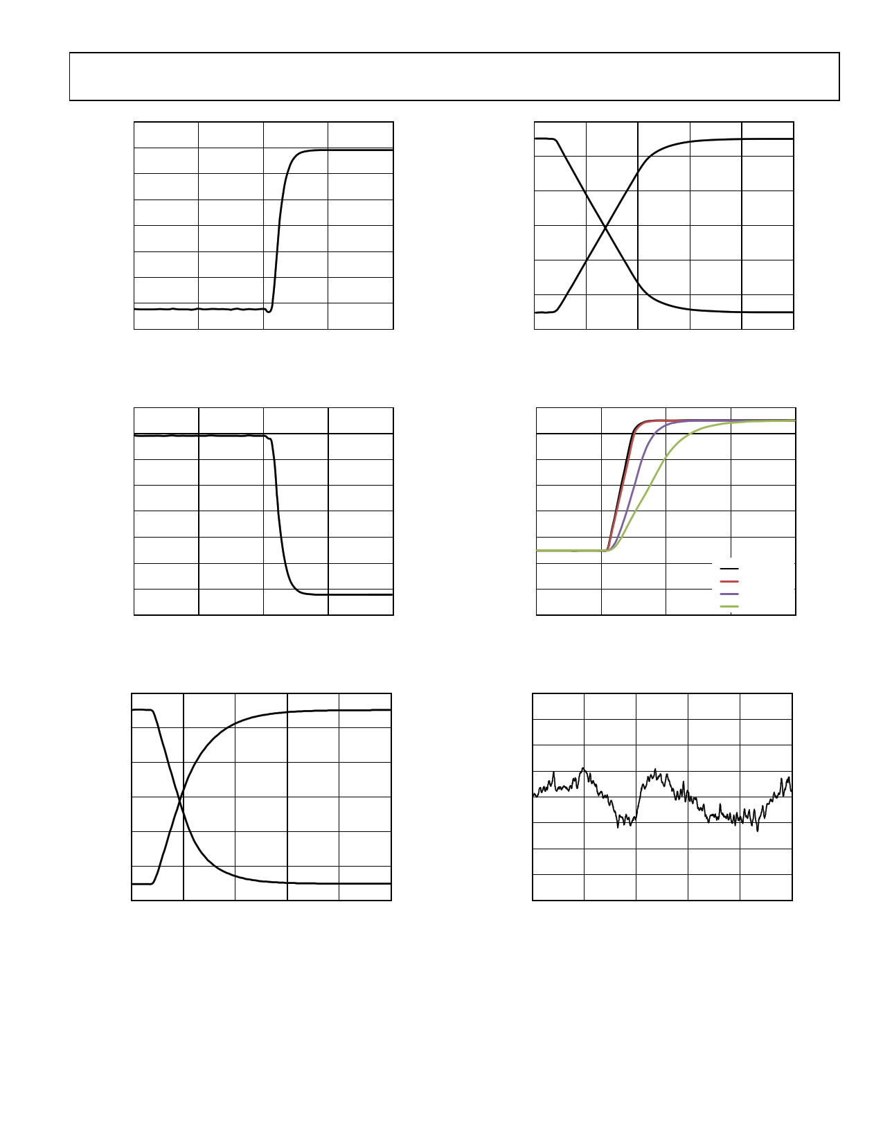
Figure 16. DAC Settling Time (100 Code Change, Rising Edge)
2.58
2.56
2.54
2.52
2.50
2.48
2.46
2.44
2.42
–10
–5 0
5
TIME (µs)
10
Figure 17. DAC Settling Time (100 Code Change, Falling Edge)
2.00
1.75
RL = 2kΩ
CL = 200pF
1.50
1.25
1.00
0.75
0.50
012345
TIME (µs)
Figure 18. DAC Settling Time, Output Range = 0 V to VREF
AD5593R
4.0
3.5
RL = 2kΩ
CL = 200pF
3.0
2.5
2.0
1.5
1.0
012345
TIME (µs)
Figure 19. DAC Settling Time, Output Range = 0 V to 2 × VREF
4.0
3.5
3.0
2.5
2.0
1.5
1.0
0.5
0
–5
0nF LOAD
10nF LOAD
22nF LOAD
47nF LOAD
0 5 10
TIME (µs)
15
Figure 20. DAC Settling Time vs. Capacitive Load
200
150
100
50
0
–50
–100
–150
–200
0
2468
TIME (Seconds)
Figure 21. DAC 1/f Noise with External Reference
10
Rev. 0 | Page 11 of 28
11 Page | ||
| Páginas | Total 28 Páginas | |
| PDF Descargar | [ Datasheet AD5593R.PDF ] | |
Hoja de datos destacado
| Número de pieza | Descripción | Fabricantes |
| AD5593R | Configurable ADC/DAC | Analog Devices |
| Número de pieza | Descripción | Fabricantes |
| SLA6805M | High Voltage 3 phase Motor Driver IC. |
Sanken |
| SDC1742 | 12- and 14-Bit Hybrid Synchro / Resolver-to-Digital Converters. |
Analog Devices |
|
DataSheet.es es una pagina web que funciona como un repositorio de manuales o hoja de datos de muchos de los productos más populares, |
| DataSheet.es | 2020 | Privacy Policy | Contacto | Buscar |
