|
|
|
PDF ZL9101M Data sheet ( Hoja de datos )
| Número de pieza | ZL9101M | |
| Descripción | Digital DC/DC PMBus 12A Module | |
| Fabricantes | Intersil | |
| Logotipo | ||
Hay una vista previa y un enlace de descarga de ZL9101M (archivo pdf) en la parte inferior de esta página. Total 17 Páginas | ||
|
No Preview Available !
Digital DC/DC PMBus 12A Module
ZL9101M
The ZL9101M is a 12A variable output step-down
PMBus-compliant digital power supply. Included in the module
is a high performance digital PWM controller, power MOSFETs,
an inductor, and all the passive components required for a
complete DC/DC power solution. The ZL9101M operates over
a wide input voltage range and supports an output voltage
range of 0.6V to 4V, which can be set by external resistors or
via PMBus. This high efficiency power module is capable of
delivering 12A. Only bulk input and output capacitors are
needed to finish the design. The output voltage can be
precisely regulated to as low as 0.6V with ±1% output voltage
regulation over line, load, and temperature variations.
The ZL9101M features internal compensation, internal
soft-start, auto-recovery overcurrent protection, an enable
option, and pre-biased output start-up capabilities.
The ZL9101M is packaged in a thermally enhanced, compact
(15mmx15mm) and low profile (3.5mm) over-molded QFN
package module suitable for automated assembly by standard
surface mount equipment. The ZL9101M is Pb-free and RoHS
compliant.
Features
• Complete Digital Switch Mode Power Supply
• Fast Transient Response
• External Synchronization
• Output Voltage Tracking
• Current Sharing
• Programmable Soft-start Delay and Ramp
• Overcurrent/Undercurrent Protection
• PMBus Compliant
Applications
• Server, Telecom, and Datacom
• Industrial and Medical Equipment
• General Purpose Point of Load
Related Literature
• See AN2033, “Zilker Labs PMBus Command Set - DDC
Products”
• See AN2034, “Configuring Current Sharing on the ZL2004
and ZL2006”
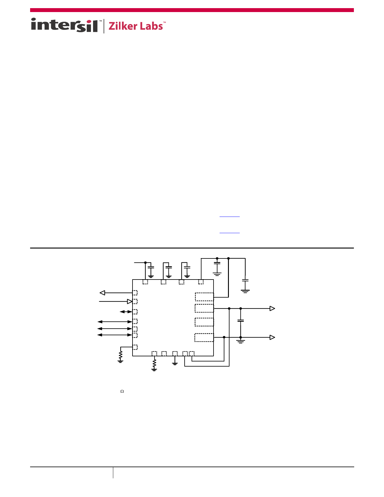
VDRV
4.5V TO 6.5V
10µF
16V
4.7µF
16V
10µF
4.7µF 16V
16V
POWER GOOD OUTPUT
ENABLE
Ext Sync
DDC Bus 2
I2C/SMBus 1
PG
EN
SYNC
DDC
SCL
SDA
SA
ZL9101M
VIN
(EPAD)
VOUT
(EPAD)
SW
(EPAD)
PGND
(EPAD)
VIN
4.5V TO 13.2V
2 x 22µF
16V
VOUT
3 x 47µF 3
16V
RTN
Notes:
1. The I2C/SMBus requires pull-up resistors. Please refer to the I2C/SMBus specifications for more details.
2. The DDC bus requires a pull-up resistor. The resistance will vary based on the capacitive loading of the bus (and on the number of
devices connected). The 10k default value, assuming a maximum of 100pF per device, provides the necessary 1µs pull-up rise time.
Please refer to the Digital-DC Bus section for more details.
3. Additional capacitance may be required to meet specific transient response targets
4. The VR, V25, VDRV, and VDD capacitors should be placed no further than 0.5 cm from the pin.
FIGURE 1. 12A APPLICATION CIRCUIT
NOTE: Figure 1 represents a typical implementation of the ZL9101M. For PMBus operation, it is recommended to tie the enable pin (EN) to SGND.
April 8, 2011
FN7669.2
1 CAUTION: These devices are sensitive to electrostatic discharge; follow proper IC Handling Procedures.
1-888-INTERSIL or 1-888-468-3774 | Intersil (and design) is a registered trademark of Intersil Americas Inc.
Copyright Intersil Americas Inc. 2010, 2011. All Rights Reserved
All other trademarks mentioned are the property of their respective owners.
Free Datasheet http://www.datasheet4u.com/
1 page 
ZL9101M
Absolute Maximum Ratings (Note 4)
DC Supply Voltage for VDD Pin . . . . . . . . . . . . . . . . . . . . . . . . -0.3V to 15.7V
Input Voltage for VIN Pin . . . . . . . . . . . . . . . . . . . . . . . . . . . . . -0.3V to 15.7V
MOSFET Drive Reference for VR Pin . . . . . . . . . . . . . . . . . . . . -0.3V to 6.5V
2.5V Logic Reference for V25 Pin. . . . . . . . . . . . . . . . . . . . . . . . . -0.3V to 3V
MOSFET Driver Power for VDRV Pin . . . . . . . . . . . . . . . . . . . . . .-0.3V to 7.5V
Logic I/O Voltage for DDC, EN,
FB+, FB-, PG, SA, SCL, SDA,SYNC, VSET Pins . . . . . . . . . . . . . . . -0.3V to 6V
ESD Rating
Human Body Model (Tested per JESD22-A114F) . . . . . . . . . . . . . . 2000V
Machine Model (Tested per JESD22-A115C) . . . . . . . . . . . . . . . . . . 200V
Charged Device Model (Tested per JESD22-C110D) . . . . . . . . . . . 1000V
Latch Up (Tested per JESD78C; Class 2, Level A) . . . . . . . . . . . . . . . 100mA
Thermal Information
Thermal Resistance (Typical)
θJA (°C/W) θJC (°C/W)
QFN Package (Notes 7, 8) . . . . . . . . . . . . . . 11.5
2.2
Junction Temperature . . . . . . . . . . . . . . . . . . . . . . . . . . . . .-55°C to +150°C
Storage Temperature . . . . . . . . . . . . . . . . . . . . . . . . . . . . . .-55°C to +150°C
Pb-Free Reflow Profile . . . . . . . . . . . . . . . . . . . . . . . . . . . . . . . see link below
http://www.intersil.com/pbfree/Pb-FreeReflow.asp
Recommended Operating Conditions
Input Supply Voltage Range, VIN . . . . . . . . . . . . . . . . . . . . . . . 4.5V to 13.2V
Input Supply For Controller, VDD (Note 5) . . . . . . . . . . . . . . . . 4.5V to 13.2V
Driver Supply Voltage, VDRV . . . . . . . . . . . . . . . . . . . . . . . . . . . . 4.5V to 6.5V
Output Voltage Range, VOUT (Note 6). . . . . . . . . . . . . . . . . . . . . 0.54V to 4V
Output Current Range, IOUT(DC) . . . . . . . . . . . . . . . . . . . . . . . . . . . 0A to 15A
Operating Junction Temperature Range, TJ. . . . . . . . . . . . . . . . . . . -40°C to +125°C
CAUTION: Do not operate at or near the maximum ratings listed for extended periods of time. Exposure to such conditions may adversely impact product
reliability and result in failures not covered by warranty.
NOTES:
4. Voltage measured with respect to SGND
5. VIN supplies the power FETs. VDD supplies the controller. VIN can be tied to VDD. For VDD ≤ 5.5V, VDD should be tied to VR.
6. Includes ±10% margin limits.
7. θJA is simulated in free air with device mounted on a four-layer FR-4 test board (76.2 x 114.3 x 1.6mm) with 80%-coverage, 2-ounce Cu on top and
bottom layers, plus two, buried, one-ounce Cu layers with coverage across the entire test board area. Multiple vias were used, with via
diameter = 0.3mm on 1.2mm pitch.
8. For θJC, the “case” temperature is measured at the center of the package underside.
Electrical Specifications VDD = 12 V, TA = -40°C to +85°C unless otherwise noted. Typical values are at TA = 25°C. Boldface limits apply
over the operating temperature range, -40°C to +85°C.
PARAMETER
CONDITIONS
MIN TYP MAX
(Note 9) (Note 10) (Note 9) UNIT
INPUT AND SUPPLY CHARACTERISTICS
Input Bias Supply Current, IDD
fSW = 615kHz, No load
– 20 40 mA
Input Bias Shutdown Current, IDDS
Input Supply Current, IVIN
Driver Supply Current, IVDRV
VR Reference Output Voltage (Note 11)
V25 Reference Output Voltage (Note 11)
OUTPUT CHARACTERISTICS
Line Regulation Accuracy, ΔVOUT/ΔVIN
(Note 12)
Load Regulation Accuracy, ΔVOUT/ΔIOUT
(Note 12)
Peak-to-peak Output Ripple Voltage, ΔVOUT
(Note 12)
Soft-start Delay Duration Range (Notes 11, 13)
Soft-start Delay Duration Accuracy (Note 11)
Soft-start Ramp Duration Range (Note 11)
EN = 0 V
No I2C/SMBus activity
VIN = 13.2V, IOUT = 15A, VOUT = 1.2V
Not switching
VDD > 6V, IVR < 20mA
VR > 3V, IV25 < 20mA
VOUT = 1.2V, IOUT = 0A, VIN = 5V to 13.2V
IOUT = 0A to 12A, VOUT = 1.2V
IOUT = 12A, VOUT = 1.2V, COUT = 3000µF
Set using I2C/SMBus
Turn-on delay (precise mode) (Notes 13, 14)
Turn-on delay (normal mode) (Note 15)
Turn-off delay (Note 15)
Set using I2C
– 9.5 12 mA
– 1.5 2 A
– 190 220 µA
4.5 5.2 5.7 V
2.25 2.5 2.75 V
– 0.5 – %
– 0.5 – %
– 6 – mV
2 – 200 ms
– ±0.25 - ms
– -0.25/+4 -
ms
– -0.25/+4 -
ms
0 – 200 ms
5 FN7669.2
April 8, 2011
Free Datasheet http://www.datasheet4u.com/
5 Page 
ZL9101M
duty cycle to match the original target voltage and the output will
ramp down to the preconfigured output voltage.
If a pre-bias voltage higher than the overvoltage limit exists, the
device will not initiate a turn-on sequence and will declare an
overvoltage fault condition to exist. In this case, the device will
respond based on the output overvoltage fault response method
that has been selected. See “Output Overvoltage Protection” on
page 10 for response options due to an overvoltage condition.
Note that pre-bias protection is not offered for current sharing
groups that also have tracking enabled.
Output Overcurrent Protection
The ZL9101M can protect the power supply from damage if the
output is shorted to ground or if an overload condition is imposed
on the output. The following overcurrent protection response
options are available:
1. Initiate a shutdown and attempt to restart an infinite number
of times with a preset delay period between attempts.
2. Initiate a shutdown and attempt to restart a preset number of
times with a preset delay period between attempts.
3. Continue operating for a given delay period, followed by
shutdown if the fault still exists.
4. Continue operating through the fault (this could result in
permanent damage to the power supply).
5. Initiate an immediate shutdown.
The default response from an overcurrent fault is an immediate
shutdown of the controller. The controller will continuously check
for the presence of the fault condition, and if the fault condition
no longer exists the device will be re-enabled.
Please refer to Application Note AN2033 for details on how to
select specific overcurrent fault response options via I2C/SMBus.
Thermal Overload Protection
The ZL9101M includes a thermal sensor that continuously
measures the internal temperature of the module and shuts
down the controller when the temperature exceeds the preset
limit. The default temperature limit is set to +125°C in the
factory, but the user may set the limit to a different value if
desired. See Application Note AN2033 for details. Note that
setting a higher thermal limit via the I2C/SMBus interface may
result in permanent damage to the controller. Once the module
has been disabled due to an internal temperature fault, the user
may select one of several fault response options as follows:
1. Initiate a shutdown and attempt to restart an infinite number
of times with a preset delay period between attempts.
2. Initiate a shutdown and attempt to restart a preset number of
times with a preset delay period between attempts.
3. Continue operating for a given delay period, followed by
shutdown if the fault still exists.
4. Continue operating through the fault (this could result in
permanent damage to the power supply).
5. Initiate an immediate shutdown.
If the user has configured the module to restart, the controller
will wait the preset delay period (if configured to do so) and will
then check the module temperature. If the temperature has
dropped below a threshold that is approximately +15 °C lower
than the selected temperature fault limit, the controller will
attempt to re-start. If the temperature still exceeds the fault limit
the controller will wait the preset delay period and retry again.
The default response from a temperature fault is an immediate
shutdown of the module. The controller will continuously check
for the fault condition, and once the fault has cleared the
ZL9101M will be re-enabled.
Please refer to Application Note AN2033 for details on how to
select specific temperature fault response options via
I2C/SMBus.
I2C/SMBus Communications
The ZL9101M provides an I2C/SMBus digital interface that
enables the user to configure all aspects of the module operation
as well as monitor the input and output parameters. The
ZL9101M can be used with any I2C host device. In addition, the
module is compatible with SMBus version 2.0. Pull-up resistors
are required on the I2C/SMBus as specified in the SMBus 2.0
specification. The ZL9101M accepts most standard PMBus
commands. When controlling the device with PMBus commands,
it is recommended that the enable pin is tied to SGND.
I2C/SMBus Module Address Selection
Each module must have its own unique serial address to
distinguish between other devices on the bus. The module
address is set by connecting a resistor between the SA pin and
SGND. Table 2 lists the available module addresses.
TABLE 2. SMBus ADDRESS RESISTOR SELECTION
RSA0
10
11
12.1
13.3
14.7
16.2
17.8
19.6
21.5
23.7
26.1
28.7
31.6
34.8
38.3
42.2
46.4
51.1
56.2
SMBus Address
0x19
0x1A
0x1B
0x1C
0x1D
0x1E
0x1F
0x20
0x21
0x22
0x23
0x24
0x25
0x26
0x27
0x28
0x29
0x2A
0x2B
11
FN7669.2
April 8, 2011
Free Datasheet http://ww
11 Page | ||
| Páginas | Total 17 Páginas | |
| PDF Descargar | [ Datasheet ZL9101M.PDF ] | |
Hoja de datos destacado
| Número de pieza | Descripción | Fabricantes |
| ZL9101M | Digital DC/DC PMBus 12A Module | Intersil |
| Número de pieza | Descripción | Fabricantes |
| SLA6805M | High Voltage 3 phase Motor Driver IC. |
Sanken |
| SDC1742 | 12- and 14-Bit Hybrid Synchro / Resolver-to-Digital Converters. |
Analog Devices |
|
DataSheet.es es una pagina web que funciona como un repositorio de manuales o hoja de datos de muchos de los productos más populares, |
| DataSheet.es | 2020 | Privacy Policy | Contacto | Buscar |