|
|
|
PDF LTM9012 Data sheet ( Hoja de datos )
| Número de pieza | LTM9012 | |
| Descripción | 125Msps ADC | |
| Fabricantes | Linear Technology | |
| Logotipo | ||
Hay una vista previa y un enlace de descarga de LTM9012 (archivo pdf) en la parte inferior de esta página. Total 28 Páginas | ||
|
No Preview Available !
Features
n 4-Channel Simultaneous Sampling ADC with
Integrated, Fixed Gain, Differential Drivers
n 68.3dB SNR
n 78dB SFDR
n Low Power: 1.27W Total, 318mW per Channel
n 1.8V ADC Core and 3.3V Analog Input Supply
n Serial LVDS Outputs: 1 or 2 Bits per Channel
n Shutdown and Nap Modes
n 11.25mm × 15mm BGA Package
Applications
n Industrial Imaging
n Medical Imaging
n Multichannel Data Acquisition
n Nondestructive Testing
L, LT, LTC, LTM, Linear Technology, the Linear logo and µModule are registered trademarks of
Linear Technology Corporation. All other trademarks are the property of their respective owners.
LTM9012
Quad 14-Bit, 125Msps ADC
with Integrated Drivers
Description
The LTM®9012 is a 4-channel, simultaneous sampling
14-bit µModule® analog-to-digital converter (ADC) with
integrated, fixed gain, differential ADC drivers. The low
noise amplifiers are suitable for single-ended drive and
pulse train signals such as imaging applications. Each
channel includes a lowpass filter between the driver out-
put and ADC input.
DC specs include ±1.2LSB INL (typ), ±0.3LSB DNL (typ)
and no missing codes over temperature. The transition
noise is a low 1.2LSBRMS.
The digital outputs are serial LVDS and each channel out-
puts two bits at a time (2-lane mode). At lower sampling
rates there is a one bit option (1-lane mode). The LVDS
drivers have optional internal termination and adjustable
output levels to ensure clean signal integrity.
The ENC+ and ENC– inputs may be driven differentially
or single-ended with a sine wave, PECL, LVDS, TTL or
CMOSwww.DataSheet.net/ inputs. An internal clock duty cycle stabilizer al-
lows high performance at full speed for a wide range of
clock duty cycles.
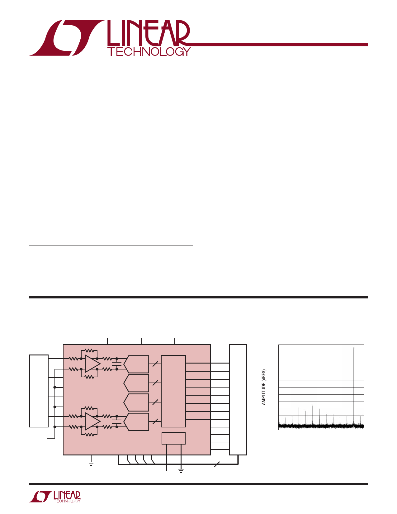
Typical Application
Single-Ended Sensor Digitization
3.3V 1.8V 1.8V
IMAGE
SENSOR
VREF
VCC
VDD
OVDD
LTM9012
PIPELINE 14
ADC
DATA
SERIALIZER
CHANNEL 1
•
•
PIPELINE 14
ADC
ENCODER
AND
LVDS
DRIVERS
CHANNEL 2
•
PIPELINE 14
CHANNEL 3
ADC
PIPELINE 14
ADC
INTERNAL
REFERENCE & SUPPLY
BYPASS CAPACITORS
SCK SDI SDO CS PAR/SER
PLL
ENC+
CHANNEL 4
ENC–
FR+
FR–
DCO+
DCO–
FPGA
ENCODE CLOCK
9012 TA01a
LTM9012, 125Msps, 70MHz FFT
0
–10
–20
–30
–40
–50
–60
–70
–80
–90
–100
–110
–120
0
5 10 15 20 25 30 35 40 45 50 55 60
FREQUENCY (MHz)
9012 TA01b
9012f
1
Datasheet pdf - http://www.DataSheet4U.co.kr/
1 page 
LTM9012
Power Requirements The l denotes the specifications which apply over the full operating temperature
range, otherwise specifications are at TA = 25°C. (Note 6)
SYMBOL
PARAMETER
CONDITIONS
MIN TYP MAX UNITS
VDD
OVDD
VCC
IVDD
IOVDD
ADC Supply Voltage
ADC Output Supply Voltage
Amplifier Supply Voltage
ADC Supply Current
ADC Output Supply Current
(Note 10)
(Note 10)
(Note 10)
Sine Wave Input
2-Lane Mode, 1.75mA Mode
2-Lane Mode, 3.5mA Mode
l 1.7
l 1.7
l 2.7
l
l
l
1.8 1.9
1.8 1.9
3.3 3.6
298 320
27 31
49 54
V
V
V
mA
mA
mA
IVCC
PDISS
Amplifier Supply Current
2-Lane Mode, 1.75mA Mode
2-Lane Mode, 3.5mA Mode
l
208 224
mA
l
1271 1473
mW
l
1311 1517
mW
PSLEEP
PNAP
PDIFFCLK
Power Decrease with Single-Ended
Encode Mode Enabled
3 mW
85 mW
20 mW
Timing Characteristics The l denotes the specifications which apply over the full operating temperature
range, otherwise specifications are at TA = 25°C. (Note 6)
SYMBOL PARAMETER
CONDITIONS
MIN TYP MAX UNITS
fS
Sampling Frequency
(Note 10, Note 11)
tENCL
ENC Low Time (Note 9)
Duty Cycle Stabilizer Off
Duty Cycle Stabilizer On
l5
125 MHz
l 3.8 4 100 ns
l2
4 100 ns
tENCH
ENC High Time (Note 9)
Duty Cycle Stabilizer Off
Duty Cycle Stabilizer On
www.DataSheet.net/
l 3.8
l2
4 100 ns
4 100 ns
tAP Sample-and-Hold
Acquisition Delay Time
0 ns
Digital Data Outputs (RTERM = 100Ω Differential, CL = 2pF to GND on Each Output)
tSER Serial Data Bit Period 2-Lanes, 16-Bit Serialization
2-Lanes, 14-Bit Serialization
2-Lanes, 12-Bit Serialization
1-Lane, 16-Bit Serialization
1-Lane, 14-Bit Serialization
1-Lane, 12-Bit Serialization
tFRAME
tDATA
tPD
tR
tF
FR to DCO Delay
DATA to DCO Delay
Propagation Delay
Output Rise Time
Output Fall Time
DCO Cycle-Cycle Jitter
Pipeline Latency
(Note 9)
(Note 9)
(Note 9)
Data, DCO, FR, 20% to 80%
Data, DCO, FR, 20% to 80%
tSER = 1ns
1/(8 • fS)
1/(7• fS)
111///(((11646•••fffSSS)))
1/(12• fS)
l 0.35 • tSER
0.5 • tSER
0.65 • tSER
l 0.35 • tSER
0.5 • tSER
0.65 • tSER
l 0.7n + 2 • tSER 1.1n + 2 • tSER 1.5n + 2 • tSER
0.17
sec
sec
sec
sec
sec
sec
sec
sec
sec
ns
0.17 ns
60 psP-P
6 Cycles
SPI Port Timing (Note 9)
tSCK SCK Period
Write Mode
Read Back Mode, CSDO = 20pF, RPULLUP = 2k
l
l
40
250
tS CS to SCK Setup Time
l5
tH SCK to CS Setup Time
l5
tDS SDI Setup Time
l5
tDH SDI Hold Time
l5
tDO
SCK Falling to SDO Valid Read Back Mode, CSDO = 20pF, RPULLUP = 2k
l
ns
ns
ns
ns
ns
ns
125 ns
9012f
5
Datasheet pdf - http://www.DataSheet4U.co.kr/
5 Page 
LTM9012
Pin Functions
VCC1 (H10, H13): Channel 1 Amplifier Supply. VCC is
internally bypassed to ground with 0.1µF in parallel with
0.01µF ceramic capacitors, additional bypass capacitance
is optional. The recommended operating voltage is 3.3V.
VCC2 (C8, C12): Channel 2 Amplifier Supply. VCC is in-
ternally bypassed to ground with 0.1µF in parallel with
0.01µF ceramic capacitors, additional bypass capacitance
is optional. The recommended operating voltage is 3.3V.
VCC3 (C2, C6): Channel 3 Amplifier Supply. VCC is in-
ternally bypassed to ground with 0.1µF in parallel with
0.01µF ceramic capacitors, additional bypass capacitance
is optional. The recommended operating voltage is 3.3V.
VCC4 (H1, H4): Channel 4 Amplifier Supply. VCC is in-
ternally bypassed to ground with 0.1µF in parallel with
0.01µF ceramic capacitors, additional bypass capacitance
is optional. The recommended operating voltage is 3.3V.
VDD (N4, N5, N9, N10): ADC Analog Supply. VDD is inter-
nally bypassed to ground with 0.1µF ceramic capacitors,
additional bypass capacitance is optional. The recom-
mended operating voltage is 1.8V.
OVDD (R7, R8, S8): ADC Digital Output Supply. OVDD
is internally bypassed to ground with 0.1µF ceramic ca-
pacitors, additional bypass capacitance is optional. The
recommended operating voltage is 1.8V.
GND: Ground. Use multiple vias close to pins.
CH1+ (A11): Channel 1 Noninverting Analog Input.
CH1– (A12): Channel 1 Inverting Analog Input.
CH2+ (A8): Channel 2 Noninverting Analog Input.
CH2– (A9): Channel 2 Inverting Analog Input.
CH3+ (A5): Channel 3 Noninverting Analog Input.
CH3– (A6): Channel 3 Inverting Analog Input.
CH4+ (A2): Channel 4 Noninverting Analog Input.
CH4– (A3): Channel 4 Inverting Analog Input.
SHDN1 (G11): Channel 1 Amplifier Shutdown. Connect-
ing SHDN1 to VCC or floating results in normal (active)
operating mode. Connecting SHDN1 to GND results in a
low power shutdown state on amplifier 1.
SHDN2 (D9): Channel 2 Amplifier Shutdown. Connect-
ing SHDN2 to VCC or floating results in normal (active)
operating mode. Connecting SHDN2 to GND results in a
low power shutdown state on amplifier 2.
SHDN3 (D3): Channel 3 Amplifier Shutdown. Connect-
ing SHDN3 to VCC or floating results in normal (active)
operating mode. Connecting SHDN3 to GND results in a
low power shutdown state on amplifier 3.
SHDN4 (G1): Channel 4 Amplifier Shutdown. Connect-
ing SHDN4 to VCC or floating results in normal (active)
operating mode. Connecting SHDN4 to GND results in a
low power shutdown state on amplifier 4.
ENC+ (N1): Encode Input. Conversion starts on the rising
edge.
ENC– (P1): Encode Complement Input. Conversion starts
on the falling edge.
CS (P4): In serial programming mode, (PAR/SER = 0V),
CS is the serial interface chip select input. When CS is
low, SCK is enabled for shifting data on SDI into the mode
control registers. In the parallel programming mode (PAR/
SER = VDD), CS selects 2-lane or 1-lane output mode. CS
can be driven with 1.8V to 3.3V logic.
www.DataSheet.net/
SCK (P5): In serial programming mode, (PAR/SER =
0V), SCK is the serial interface clock input. In the parallel
programming mode (PAR/SER = VDD), SCK selects 3.5mA
or 1.75mA LVDS output currents. SCK can be driven with
1.8V to 3.3V logic.
SDI (P3): In serial programming mode, (PAR/SER = 0V),
SDI is the serial interface data Input. Data on SDI is clocked
into the mode control registers on the rising edge of SCK.
In the parallel programming mode (PAR/SER = VDD), SDI
can be used to power down the part. SDI can be driven
with 1.8V to 3.3V logic.
SDO (P9): In serial programming mode, (PAR/SER = 0V),
SDO is the optional serial interface data output. Data on
SDO is read back from the mode control registers and can
be latched on the falling edge of SCK. SDO is an open-
drain NMOS output that requires an external 2k pull-up
resistor to 1.8V – 3.3V. If read back from the mode control
registers is not needed, the pull-up resistor is not neces-
sary and SDO can be left unconnected. In the parallel
programming mode (PAR/SER = VDD), SDO is an input
that enables internal 100Ω termination resistors. When
used as an input, SDO can be driven with 1.8V to 3.3V
logic through a 1k series resistor.
9012f
11
Datasheet pdf - http://www.DataSheet4U.co.kr/
11 Page | ||
| Páginas | Total 28 Páginas | |
| PDF Descargar | [ Datasheet LTM9012.PDF ] | |
Hoja de datos destacado
| Número de pieza | Descripción | Fabricantes |
| LTM9010-14 | 125Msps/105Msps/ 80Msps Low Power Octal ADCs | Linear Technology |
| LTM9011-14 | 125Msps/105Msps/ 80Msps Low Power Octal ADCs | Linear Technology |
| LTM9012 | 125Msps ADC | Linear Technology |
| Número de pieza | Descripción | Fabricantes |
| SLA6805M | High Voltage 3 phase Motor Driver IC. |
Sanken |
| SDC1742 | 12- and 14-Bit Hybrid Synchro / Resolver-to-Digital Converters. |
Analog Devices |
|
DataSheet.es es una pagina web que funciona como un repositorio de manuales o hoja de datos de muchos de los productos más populares, |
| DataSheet.es | 2020 | Privacy Policy | Contacto | Buscar |