|
|
|
PDF CYU01M16SCCU Data sheet ( Hoja de datos )
| Número de pieza | CYU01M16SCCU | |
| Descripción | 16-Mbit (1M x 16) Pseudo Static RAM | |
| Fabricantes | Cypress Semiconductor | |
| Logotipo | ||
Hay una vista previa y un enlace de descarga de CYU01M16SCCU (archivo pdf) en la parte inferior de esta página. Total 12 Páginas | ||
|
No Preview Available !
PRELIMINARY
CYU01M16SCCU
MoBL3™
16-Mbit (1M x 16) Pseudo Static RAM
Features
• Wide voltage range: 2.2V–3.6V
• Access Time: 70 ns
• Ultra-low active power
— Typical active current: 3 mA @ f = 1 MHz
— Typical active current: 18 mA @ f = fmax
• Ultra low standby power
• 16-word Page Mode
• Automatic power-down when deselected
• CMOS for optimum speed/power
• Offered in a 48-ball BGA Package
• Operating Temperature: –40°C to +85°C
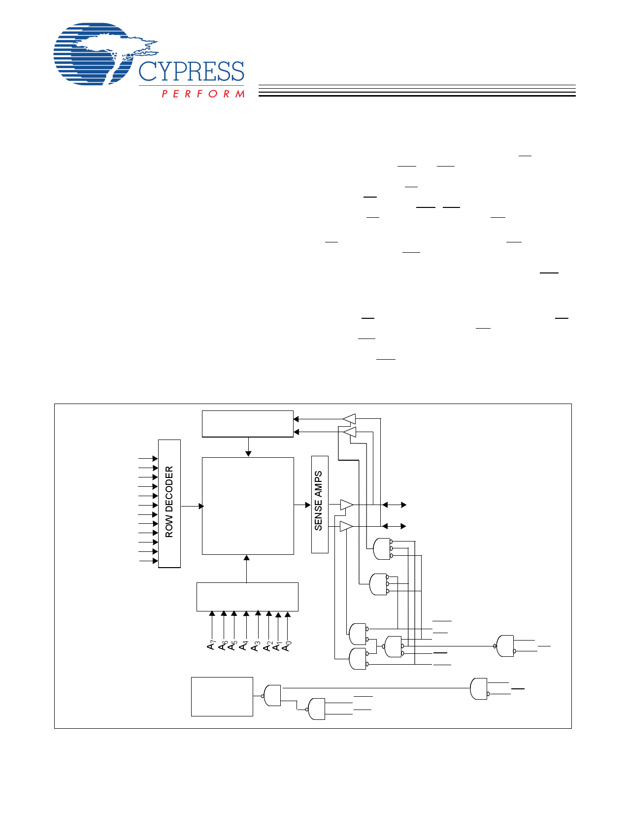
Functional Description[1]
The CYU01M16SCCU is a high-performance CMOS Pseudo
Static RAM organized as 1M words by 16 bits that supports an
asynchronous memory interface. This device features
advanced circuit design to provide ultra-low active current.
This is ideal for providing More Battery Life™ (MoBL®) in
Logic Block Diagram
DATA IN DRIVERS
portable applications such as cellular telephones. The device
can be put into standby mode when deselected (CE1 HIGH or
CE2 LOW or both BHE and BLE are HIGH). The input/output
pins (I/O0 through I/O15) are placed in a high-impedance state
when: deselected (CE1 HIGH or CE2 LOW), outputs are
disabled (OE HIGH), both Byte High Enable and Byte Low
Enable are disabled (BHE, BLE HIGH), or during a write
operation (CE1 LOW and CE2 HIGH and WE LOW).
Writing to the device is accomplished by taking Chip Enable
(CE1 LOW and CE2 HIGH) and Write Enable (WE) input LOW.
If Byte Low Enable (BLE) is LOW, then data from I/O pins (I/O0
through I/O7), is written into the location specified on the
address pins (A0 through A19). If Byte High Enable (BHE) is
LOW, then data from I/O pins (I/O8 through I/O15) is written into
the location specified on the address pins (A0 through A19).
Reading from the device is accomplished by taking Chip
Enables (CE1 LOW and CE2 HIGH) and Output Enable (OE)
LOW while forcing the Write Enable (WE) HIGH. If Byte Low
Enable (BLE) is LOW, then data from the memory location
specified by the address pins will appear on I/O0 to I/O7. If Byte
High Enable (BHE) is LOW, then data from memory will appear
on I/O8 to I/O15. Refer to the truth table for a complete
description of read and write modes.
AAAAAAAAAAA11111111141088326579
1M x 16
RAM Array
A19
I/O0–I/O7
I/O8–I/O15
COLUMN DECODER
Power -Down
Circuit
BHE
BLE
BHE
WE
OE
BLE
CE2
CE1
CE2
CE1
Note:
1. For best-practice recommendations, please refer to the Cypress application note “System Design Guidelines” on http://www.cypress.com.
Cypress Semiconductor Corporation • 198 Champion Court • San Jose, CA 95134-1709 • 408-943-2600
www.DDaotacSuhmeeetn4Ut #.n:e3t 8-05601 Rev. *B
Revised January 25, 2006
1 page 
PRELIMINARY
CYU01M16SCCU
MoBL3™
AC Test Loads and Waveforms
VCC
OUTPUT
R1
30 pF
INCLUDING
JIG AND
SCOPE
ALL INPUT PULSES
VCC
GND
10%
90%
90%
10%
R2 Rise Time = 1 V/ns
Fall Time = 1 V/ns
Equivalent to: THEVENIN EQUIVALENT
OUTPUT
RTH
VTH
Parameters
R1
R2
RTH
VTH
3.0V (VCC)
26000
26000
13000
1.50
Unit
Ω
Ω
Ω
V
Switching Characteristics Over the Operating Range[9, 10, 11, 15,14]
70 ns
Parameter
Description
Min.
Max.
Unit
Read Cycle
tRC [13]
Read Cycle Time
tCD Chip Deselect Time CE1 = HIGH or
CE2 =LOW, BLE/BHE High Pulse Time
tAA Address to Data Valid
tOHA
Data Hold from Address Change
tACE CE LOW to Data Valid
tDOE
tLZOE
tHZOE
tLZCE
tHZCE
OE LOW to Data Valid
OE LOW to Low Z[10, 11, 12]
OE HIGH to High Z[10, 11, 12]
CE LOW to Low Z[10, 11, 12]
CE HIGH to High Z[10, 11, 12]
tDBE
tLZBE
tHZBE
BLE/BHE LOW to Data Valid
BLE/BHE LOW to Low Z[10, 11, 12]
BLE/BHE HIGH to High Z[10, 11, 12]
Page Read Cycle
70 40000
15
70
5
70
35
5
25
10
25
70
5
25
ns
ns
ns
ns
ns
ns
ns
ns
ns
ns
ns
ns
ns
tPC Page Mode Read Cycle Time
35 40000
ns
tPA Page Mode Address Access
35 ns
Notes:
9.
Test conditions for all parameters other than tri-state parameters assume signal transition
of 0V to VCC, and output loading of the specified IOL/IOH as shown in the “AC Test Loads
time
and
of 1 ns/V, timing reference
Waveforms” section.
levels
of
VCC(typ.)/2,
input
pulse levels
10.
Agitvaennydgeivviecne.teAmll ploewra-ZturpearaanmdevtoelrtsagweillcboendmitieoanssutrHeZdCwEiitsh
laeslosathdacnaptLaZcCiEta,ntHceZBoEf
is less
30 pF
than
(3V)
tLZBE,
tHZOE
is
less
than
tLZOE,
and
tHZWE
is
less
than
tLZWE
for
any
11. tHZOE, tHZCE, tHZBE, and tHZWE transitions are measured when the outputs enter a high -impedence state.
12. High-Z and Low-Z parameters are characterized and are not 100% tested.
13.
If invalid address signals
at least once in every 40
shorter
µs.
than
min.tRC
are
continuously
repeated
for
40
µs,
the
device
needs
a
normal
read
timing
(tRC)
or
needs
to
enter
standby
state
14.
In order to achieve
going active.
70-ns
performance,
the
read
access
must
be
Chip
Enable
(CE1
or
CE2)
controlled.
That
is,
the
addresses
must
be
stable
prior
to
Chip
Enable
Document #: 38-05601 Rev. *B
Page 5 of 12
5 Page 
PRELIMINARY
CYU01M16SCCU
MoBL3™
Ordering Information
Speed
(ns)
70
Ordering Code
CYU01M16SCCU-70BVXI
Package
Name
BV48
Package Type
48-ball Fine Pitch VBGA (6 mm × 8 mm × 1 mm) (Pb-Free)
Operating
Range
Industrial
Package Diagram
TOP VIEW
A1 CORNER
12 3 4 5 6
A
B
C
D
E
F
G
H
48-ball VFBGA (6 x 8 x 1 mm) BV48
BOTTOM VIEW
A1 CORNER
Ø0.05 M C
Ø0.25 M C A B
Ø0.30±0.05(48X)
6 54 3 2 1
A
B
C
D
E
F
G
H
A
B
6.00±0.10
A 1.875
0.75
3.75
B
0.15(4X)
6.00±0.10
SEATING PLANE
C
51-85150-*D
MoBL is a registered trademark and MoBL3 and More Battery Life are trademarks of Cypress Semiconductor Corporation. All
product and company names mentioned in this document may be the trademarks of their respective holders.
Document #: 38-05601 Rev. *B
Page 11 of 12
© Cypress Semiconductor Corporation, 2006. The information contained herein is subject to change without notice. Cypress Semiconductor Corporation assumes no responsibility for the use
of any circuitry other than circuitry embodied in a Cypress product. Nor does it convey or imply any license under patent or other rights. Cypress products are not warranted nor intended to be
used for medical, life support, life saving, critical control or safety applications, unless pursuant to an express written agreement with Cypress. Furthermore, Cypress does not authorize its
products for use as critical components in life-support systems where a malfunction or failure may reasonably be expected to result in significant injury to the user. The inclusion of Cypress
products in life-support systems application implies that the manufacturer assumes all risk of such use and in doing so indemnifies Cypress against all charges.
11 Page | ||
| Páginas | Total 12 Páginas | |
| PDF Descargar | [ Datasheet CYU01M16SCCU.PDF ] | |
Hoja de datos destacado
| Número de pieza | Descripción | Fabricantes |
| CYU01M16SCCU | 16-Mbit (1M x 16) Pseudo Static RAM | Cypress Semiconductor |
| Número de pieza | Descripción | Fabricantes |
| SLA6805M | High Voltage 3 phase Motor Driver IC. |
Sanken |
| SDC1742 | 12- and 14-Bit Hybrid Synchro / Resolver-to-Digital Converters. |
Analog Devices |
|
DataSheet.es es una pagina web que funciona como un repositorio de manuales o hoja de datos de muchos de los productos más populares, |
| DataSheet.es | 2020 | Privacy Policy | Contacto | Buscar |