|
|
|
PDF 3N190 Data sheet ( Hoja de datos )
| Número de pieza | 3N190 | |
| Descripción | Amplifier | |
| Fabricantes | Micross | |
| Logotipo | ||
Hay una vista previa y un enlace de descarga de 3N190 (archivo pdf) en la parte inferior de esta página. Total 1 Páginas | ||
|
No Preview Available !
3N190
P-CHANNEL MOSFET
The 3N190 is a monolithic dual enhancement mode P-Channel Mosfet
The 3N190 is a dual enhancement mode P-Channel
Mosfet and is ideal for space constrained applications
and those requiring tight electrical matching.
The hermetically sealed TO-78 package is well suited
for high reliability and harsh environment applications.
FEATURES
DIRECT REPLACEMENT FOR INTERSIL 3N190
LOW GATE LEAKAGE CURRENT
IGSS ≤ ± 10pA
LOW TRANSFER CAPACITANCE
Crss ≤ 1.0pF
ABSOLUTE MAXIMUM RATINGS1@ 25°C (unless otherwise noted)
Maximum Temperatures
(See Packaging Information).
Storage Temperature
Operating Junction Temperature
‐65°C to +150°C
‐55°C to +135°C
Maximum Power Dissipation
3N190 Features:
Continuous Power Dissipation (one side)
Continuous Power Dissipation (one side)
300mW
525mW
Very high Input Impedance
High Gate Breakdown Voltage
Low Capacitance
MAXIMUM CURRENT
Drain to Source2
MAXIMUM VOLTAGES
Drain to Gate or Drain to Source2
Transient Gate to Source2,3
50mA
‐30V
±125V
Gate‐Gate Voltage
±80V
3N190 ELECTRICAL CHARACTERISTICS @ 25°C (unless otherwise noted)
SYMBOL
CHARACTERISTIC
MIN TYP.
MAX
UNITS
CONDITIONS
BVDSS
Drain to Source Breakdown Voltage ‐40
BVSDS
Source to Drain Breakdown Voltage ‐40
VGS
Gate to Source Voltage
‐3.0
VGS(th)
Gate to Source Threshold Voltage ‐2.0
‐2.0
IGSSR
Gate Reverse Leakage Current
‐‐
IGSSF
Forward Gate Leakage Current
‐‐
IDSS
Drain to Source Leakage Current
‐‐
ISDS
ID(on)
rDS(on)
gfs
ClickYos
Source to Drain Leakage Current
Drain Current “On”
Drain to Source “On” Resistance
Forward Transconductance4
Output Admittance
‐‐
‐5.0
‐‐
1500
‐‐
‐‐ ‐‐
‐‐ ‐‐
‐‐ ‐6.5
‐‐ ‐5.0
‐‐ ‐5.0
‐‐ 10
‐‐ ‐10
‐‐ ‐200
To‐‐ ‐400
‐‐ ‐30
‐‐ 300
‐‐ 4000
‐‐ 300
ID = ‐10µA
IS = ‐10µA, VBD = 0V
V VDS = ‐15V, ID = ‐500µA
VDS = ‐15V, ID = ‐500µA
VDS = VGS , ID = ‐10µA
VGS = 40V
VGS = ‐40V
pA VDS = ‐15V
BuyVSD = ‐15V VDB = 0
mA VDS = ‐15V, VGS = ‐10V
Ω VDS = ‐20V, ID = ‐100µA
µS VDS = ‐15V, ID = ‐5mA , f = 1kHz
Ciss
Input Capacitance
‐‐ ‐‐ 4.5
Crss
Reverse Transfer Capacitance
‐‐
‐‐
1.0
pF
VDS = ‐15V, ID = ‐5mA , f = 1MHz
Coss
Output Capacitance
‐‐ ‐‐ 3.0
MATCHING CHARACTERISTICS 3N190
SYMBOL
LIMITS
CHARACTERISTIC
MIN MAX
UNITS
CONDITIONS
gfs1/gfs2
VGS1‐2
Forward Transconductance Ratio
Gate Source Threshold Voltage
Differential5
0.85
‐‐
1.0
100
ns
mV
VDS = ‐15V, ID = ‐500µA , f = kHz
VDS = ‐15V, ID = ‐500µA
∆VGS1‐2/∆T
Gate Source Threshold Voltage
Differential Change with Temperature5
‐‐
100 µV/°C
VDS = ‐15V, ID = ‐500µA, TS = ‐55°C to +25°C
VDS = ‐15V, ID = ‐500µA, TS = +25°C to +125°C
SWITCHING CHARACTERISTICS
SYMBOL
CHARACTERISTIC
MIN
TYP
MAX
UNITS
CONDITIONS
td(on)
tr
toff
Turn On Delay Time
Turn On Rise Time
Turn Off Time
‐‐ ‐‐ 15
‐‐ ‐‐ 30
‐‐ ‐‐ 50
ns
VDD = ‐15V, ID(on) = ‐5mA, RG = RL = 1.4KΩ
Note 1 ‐ Absolute maximum ratings are limiting values above which 3N190 serviceability may be impaired.
Note 2 – Per Transistor
Note 3 – Approximately doubles for every 10°C in TA
Note 4 – Measured at end points, TA and TB
Note 5 – Pulse: t= 300µS, Duty Cycle ≤ 3%
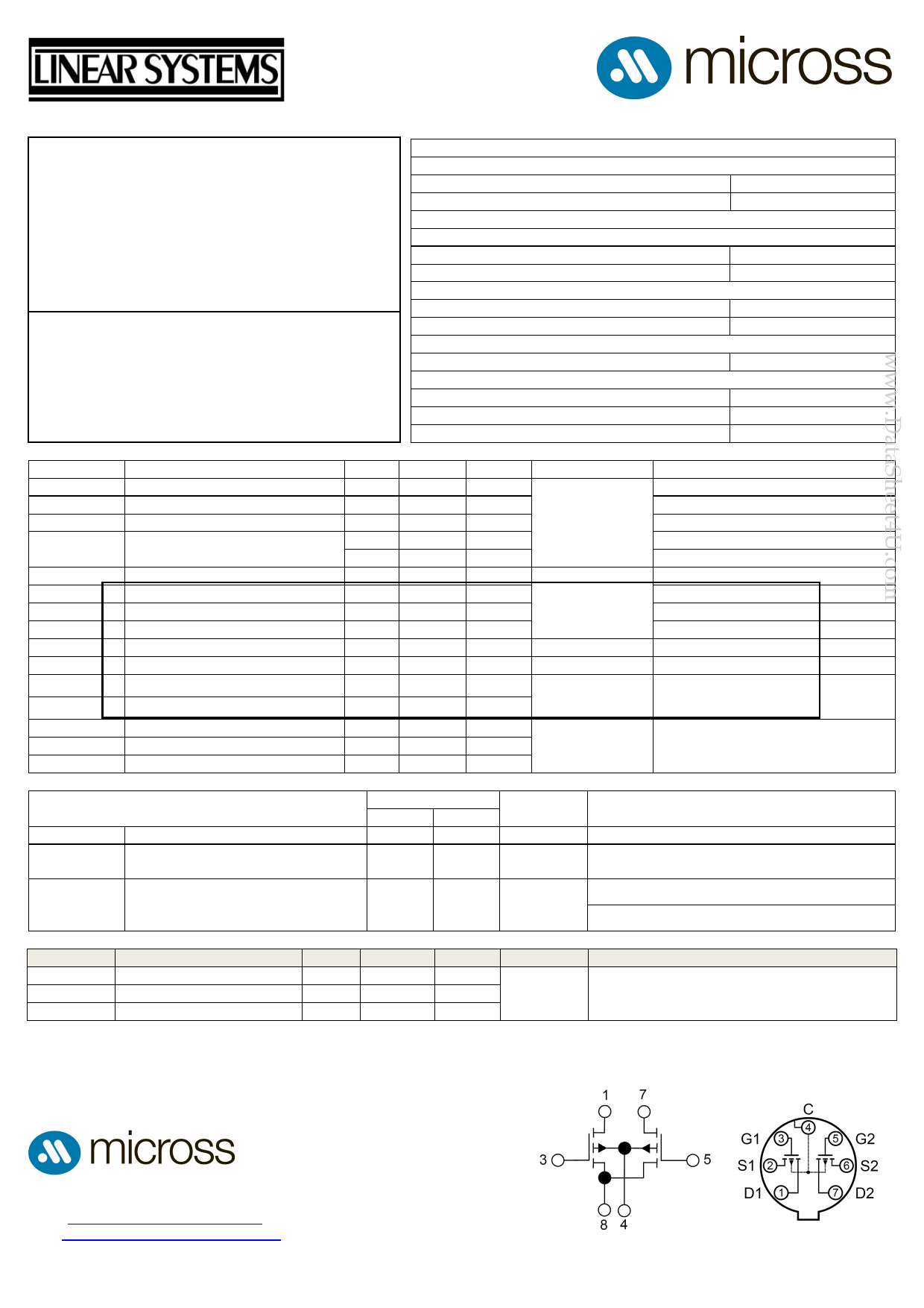
Device Schematic
TO-78 (Bottom View)
Tel: +44 1603 788967
Email: [email protected]
Web: http://www.micross.com/distribution
Available Packages:
3N190 in TO-72
3N190 in bare die.
Please contact Micross for full
package and die dimensions
Information furnished by Linear Integrated Systems and Micross Components is believed to be accurate and reliable. However, no responsibility is assumed for its use; nor for any infringement of patents or
other rights of third parties which may result from its use. No license is granted by implication or otherwise under any patent or patent rights of Linear Integrated Systems.
1 page | ||
| Páginas | Total 1 Páginas | |
| PDF Descargar | [ Datasheet 3N190.PDF ] | |
Hoja de datos destacado
| Número de pieza | Descripción | Fabricantes |
| 3N190 | Dual P-Channel Enhancement Mode MOSFET General Purpose Amplifier | Calogic LLC |
| 3N190 | P-CHANNEL DUAL MOSFET ENHANCEMENT MODE | Linear Integrated Systems |
| 3N190 | Amplifier | Micross |
| 3N190 | (3N188 - 3N191) Dual P-Channel Enhancement Mode MOSFET | Intersil |
| Número de pieza | Descripción | Fabricantes |
| SLA6805M | High Voltage 3 phase Motor Driver IC. |
Sanken |
| SDC1742 | 12- and 14-Bit Hybrid Synchro / Resolver-to-Digital Converters. |
Analog Devices |
|
DataSheet.es es una pagina web que funciona como un repositorio de manuales o hoja de datos de muchos de los productos más populares, |
| DataSheet.es | 2020 | Privacy Policy | Contacto | Buscar |