|
|
PDF MAX15040 Data sheet ( Hoja de datos )
| Número de pieza | MAX15040 | |
| Descripción | Step-Down Regulator | |
| Fabricantes | Maxim Integrated Products | |
| Logotipo |  |
|
Hay una vista previa y un enlace de descarga de MAX15040 (archivo pdf) en la parte inferior de esta página. Total 15 Páginas | ||
|
No Preview Available !
19-4426; Rev 2; 7/10
EVAALVUAAILTAIOBNLEKIT
High-Efficiency, 4A, Step-Down Regulatowwrw.wDataiSthehet4U.com
Integrated Switches in 2mm x 2mm Package
General Description
The MAX15040 high-efficiency switching regulator
delivers up to 4A load current at output voltages from
0.6V to (0.9 x VIN). The device operates from 2.4V to
3.6V, making it ideal for on-board point-of-load and
postregulation applications. Total output-voltage accu-
racy is within ±1% over load, line, and temperature.
The MAX15040 features 1MHz fixed-frequency PWM
mode operation. The high operating frequency allows
for small-size external components.
The low-resistance on-chip nMOS switches ensure high
efficiency at heavy loads while minimizing critical parasitic
inductances, making the layout a much simpler task with
respect to discrete solutions. Following a simple layout
and footprint ensures first-pass success in new designs.
The MAX15040 incorporates a high-bandwidth
(> 15MHz) voltage-error amplifier. The voltage-mode
control architecture and the voltage-error amplifier per-
mit a Type III compensation scheme to achieve maxi-
mum loop bandwidth, up to 200kHz. High loop
bandwidth provides fast transient response, resulting in
less required output capacitance and allowing for all-
ceramic capacitor designs.
The MAX15040 features an output overload hiccup pro-
tection and peak current limit on both high-side (sourc-
ing current) and low-side (sinking and sourcing current)
MOSFETs, for ultra-safe operations in case of high out-
put prebias, short-circuit conditions, severe overloads,
or in converters with bulk electrolytic capacitors.
The MAX15040 features an adjustable output voltage.
The output voltage is adjustable by using two external
resistors at the feedback or by applying an external ref-
erence voltage to the REFIN/SS input. The MAX15040
offers programmable soft-start time using one capacitor
to reduce input inrush current. A built-in thermal shut-
down protection assures safe operation under all condi-
tions. The MAX15040 is available in a 2mm x 2mm,
16-bump (4 x 4 array), 0.5mm pitch WLP package.
Applications
Server Power Supplies
Point-of-Load
ASIC/CPU/DSP Core and I/O Voltages
DDR Power Supplies
Base-Station Power Supplies
Telecom and Networking Power Supplies
RAID Control Power Supplies
Features
o Internal 15mΩ RDS(ON) MOSFETs
o Continuous 4A Output Current
o ±1% Output-Voltage Accuracy Over Load, Line,
and Temperature
o Operates from 2.4V to 3.6V Supply
o Adjustable Output from 0.6V to (0.9 x VIN)
o Adjustable Soft-Start Reduces Inrush Supply
Current
o Factory-Trimmed 1MHz Switching Frequency
o Compatible with Ceramic, Polymer, and
Electrolytic Output Capacitors
o Safe Startup into Prebias Output
o Enable Input/Power-Good Output
o Fully Protected Against Overcurrent and
Overtemperature
o Overload Hiccup Protection
o Sink/Source Current in DDR Applications
o 2mm x 2mm, 16-Bump (4 x 4 Array), 0.5mm Pitch
WLP Package
Ordering Information
PART
TEMP RANGE
PIN-PACKAGE
MAX15040EWE+
-40°C to +85°C
16 WLP
+Denotes a lead(Pb)-free/RoHS-compliant package.
Typical Operating Circuit
INPUT
2.4V TO 3.6V
IN BST
MAX15040
EN
VDD
LX
GND
OUTPUT
FB
REFIN/SS
COMP
VDD
PWRGD
GND
Pin Configuration appears at end of data sheet.
________________________________________________________________ Maxim Integrated Products 1
For pricing, delivery, and ordering information, please contact Maxim Direct at 1-888-629-4642,
or visit Maxim’s website at www.maxim-ic.com.
1 page 
High-Efficiency, 4A, Step-Down Regulatowwrw.wDataiSthehet4U.com
Integrated Switches in 2mm x 2mm Package
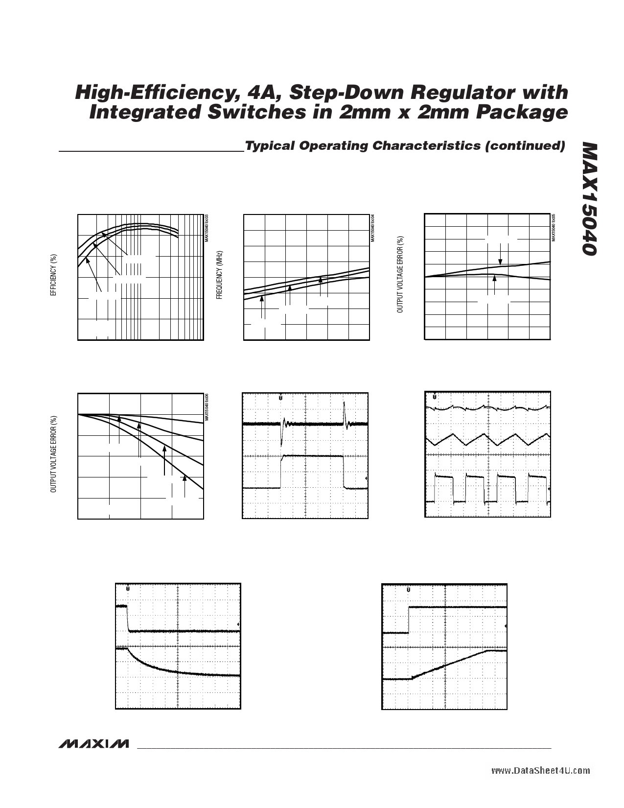
Typical Operating Characteristics (continued)
(VIN = VDD = 3.3V, output voltage = 1.8V, ILOAD = 4A, and TA = +25°C, circuit of Figure 1, unless otherwise noted.)
EFFICIENCY
vs. OUTPUT CURRENT
100
90
80 VOUT = 1.8V
70 VOUT = 1.5V
60 VOUT = 1.2V
50
VDD = 3.3V
VIN = 2.5V
40
0.1
1
OUTPUT CURRENT (A)
10
LOAD REGULATION
0.10
0
-0.10
-0.20
VOUT = 2.5V
VOUT = 1.8V
-0.30 VOUT = 1.5V
-0.40
INTERNAL REFERENCE
VOUT = 1.2V
-0.50
01234
LOAD CURRENT (A)
FREQUENCY
vs. INPUT VOLTAGE
1.20
1.15
1.10
1.05
1.00
0.95
TA = +85°C
0.90 TA = +25°C
0.85 TA = -40°C
0.80
2.4 2.6 2.8 3.0 3.2 3.4
INPUT VOLTAGE (V)
3.6
0.5
0.4
0.3
0.2
0.1
0
-0.1
-0.2
-0.3
-0.4
-0.5
2.4
LINE REGULATION
VOUT = 1.2V
VOUT = 1.8V
2.6 2.8 3.0 3.2 3.4
INPUT VOLTAGE (V)
3.6
LOAD-TRANSIENT RESPONSE
MAX15040 toc07
VOUT
AC-COUPLED
VOUT 100mV/div
ILX
SWITCHING WAVEFORMS
MAX15040 toc08
AC-COUPLED
50mV/div
2A/div
IOUT 1A/div
0
VLX 2V/div
00
40µs/div
400ns/div
SHUTDOWN WAVEFORM
MAX15040 toc09
SOFT-START WAVEFORM
MAX15040 toc10
VEN
2V/div
VEN
2V/div
00
VOUT 1V/div
0
10µs/div
IOUT = 1.8A
VOUT 1V/div
0
400µs/div
_______________________________________________________________________________________ 5
5 Page 
High-Efficiency, 4A, Step-Down Regulatowrw withw . D a t a S h e e t 4 U . c o
Integrated Switches in 2mm x 2mm Package
Shutdown Mode
Drive EN to GND to shut down the device and reduce
quiescent current to less than 0.1µA. During shutdown,
LX is high impedance. Drive EN high to enable the
MAX15040.
Thermal Protection
Thermal-overload protection limits total power dissipation
in the device. When the junction temperature exceeds TJ
= +165°C, a thermal sensor forces the device into shut-
down, allowing the die to cool. The thermal sensor turns
the device on again after the junction temperature cools
by 20°C, causing a pulsed output during continuous
overload conditions. The soft-start sequence begins after
recovery from a thermal-shutdown condition.
Applications Information
IN and VDD Decoupling
To decrease the noise effects due to the high switching
frequency and maximize the output accuracy of
the MAX15040, decouple VIN with a 22µF capacitor in
parallel with a 0.1µF capacitor from VIN to GND. Also
decouple VDD with a 1µF capacitor from VDD to GND.
Place these capacitors as close as possible to the device.
Inductor Selection
Choose an inductor with the following equation:
L = VOUT × (VIN − VOUT)
fS × VIN × LIR × IOUT(MAX)
where LIR is the ratio of the inductor ripple current to full
load current at the minimum duty cycle and fS is the
switching frequency (1MHz). Choose LIR between 20%
to 40% for best performance and stability.
Use an inductor with the lowest possible DC resistance
that fits in the allotted dimensions. Powdered iron or ferrite
core types are often the best choice for performance.
With any core material, the core must be large enough
not to saturate at the current limit of the MAX15040.
Output-Capacitor Selection
The key selection parameters for the output capacitor are
capacitance, ESR, ESL, and voltage-rating requirements.
These affect the overall stability, output ripple voltage,
and transient response of the DC-DC converter. The out-
put ripple occurs due to variations in the charge stored
in the output capacitor, the voltage drop due to the
capacitor’s ESR, and the voltage drop due to the
capacitor’s ESL. Estimate the output voltage ripple due
to the output capacitance, ESR, and ESL as follows:
VRIPPLE = VRIPPLE(C) +
VRIPPLE(ESR) + VRIPPLE(ESL)
where the output ripple due to output capacitance,
ESR, and ESL is:
VRIPPLE(C)
=
8
IP − P
x COUT
x
fS
VRIPPLE(ESR) = IP−P x ESR
VRIPPLE(ESL)
= IP−P
tON
x ESL or
VRIPPLE(ESL)
=
IP − P
tOFF
x
ESL
or whichever is higher.
The peak-to-peak inductor current (IP-P) is:
IP−P
=
VIN − VOUT
fS × L
x
VOUT
VIN
Use these equations for initial output capacitor selec-
tion. Determine final values by testing a prototype or an
evaluation circuit. A smaller ripple current results in less
output voltage ripple. Since the inductor ripple current
is a factor of the inductor value, the output voltage rip-
ple decreases with larger inductance. Use ceramic
capacitors for low ESR and low ESL at the switching
frequency of the converter. The ripple voltage due to
ESL is negligible when using ceramic capacitors.
Load-transient response depends on the selected out-
put capacitance. During a load transient, the output
instantly changes by ESR x ∆ILOAD. Before the con-
troller can respond, the output deviates further,
depending on the inductor and output capacitor val-
ues. After a short time, the controller responds by regu-
lating the output voltage back to its predetermined
value. The controller response time depends on the
closed-loop bandwidth. A higher bandwidth yields a
faster response time, preventing the output from deviat-
ing further from its regulating value. See the Compen-
sation Design section for more details.
______________________________________________________________________________________ 11
11 Page | ||
| Páginas | Total 15 Páginas | |
| PDF Descargar | [ Datasheet MAX15040.PDF ] | |
Hoja de datos destacado
| Número de pieza | Descripción | Fabricantes |
| MAX15040 | Step-Down Regulator | Maxim Integrated Products |
| MAX15041 | Step-Down DC-DC Regulator | Maxim Integrated Products |
| MAX15041 | Step-Down DC-DC Regulator | Maxim Integrated Products |
| MAX15046 | 40V High-Performance Synchronous Buck Controller | Maxim Integrated Products |
| Número de pieza | Descripción | Fabricantes |
| SLA6805M | High Voltage 3 phase Motor Driver IC. |
Sanken |
| SDC1742 | 12- and 14-Bit Hybrid Synchro / Resolver-to-Digital Converters. |
Analog Devices |
|
DataSheet.es es una pagina web que funciona como un repositorio de manuales o hoja de datos de muchos de los productos más populares, |
| DataSheet.es | 2020 | Privacy Policy | Contacto | Buscar |
