|
|
|
PDF CYW15G0401DXB Data sheet ( Hoja de datos )
| Número de pieza | CYW15G0401DXB | |
| Descripción | Transceiver | |
| Fabricantes | Cypress Semiconductor | |
| Logotipo | ||
Hay una vista previa y un enlace de descarga de CYW15G0401DXB (archivo pdf) en la parte inferior de esta página. Total 30 Páginas | ||
|
No Preview Available !
CYP15G0401DXB
CYV15G0401DXB
CYW15G0401DXB
Quad HOTLink II™ Transceiver
Features
• Second-generation HOTLink® technology
• Compliant to multiple standards
— ESCON, DVB-ASI, Fibre Channel and Gigabit
Ethernet (IEEE802.3z)
— CPRI™ compliant
www.DataSheet4U—.coCmYW15G0401DXB compliant to OBSAI-RP3
— CYV15G0401DXB compliant to SMPTE 259M and
SMPTE 292M
— 8B/10B encoded or 10-bit unencoded data
• Quad channel transceiver operates from 195 to
1500 MBaud serial data rate
— CYW15G0401DXB operates from 195 to 1540 MBaud
— Aggregate throughput of 12 GBits/second
• Selectable parity check/generate
• Selectable multi-channel bonding options
— Four 8-bit channels
— Two 16-bit channels
— One 32-bit channel
— N x 32-bit channel support (inter-chip)
• Skew alignment support for multiple bytes of offset
• Selectable input/output clocking options
• MultiFrame™ Receive Framer
— Bit and Byte alignment
— Comma or full K28.5 detect
— Single- or multi-byte framer for byte alignment
— Low-latency option
• Synchronous LVTTL parallel interface
• Optional Elasticity Buffer in Receive Path
• Optional Phase Align Buffer in Transmit Path
• Internal phase-locked loops (PLLs) with no external
PLL components
• Dual differential PECL-compatible serial inputs per
channel
— Internal DC-restoration
• Dual differential PECL-compatible serial outputs per
channel
— Source matched for 50Ω transmission lines
— No external bias resistors required
— Signaling-rate controlled edge-rates
• Compatible with
— fiber-optic modules
— copper cables
— circuit board traces
• JTAG boundary scan
• Built-In Self-Test (BIST) for at-speed link testing
• Per-channel Link Quality Indicator
— Analog signal detect
— Digital signal detect
• Low power 2.5W @ 3.3V typical
• Single 3.3V supply
• 256-ball thermally enhanced BGA
• Pb-free package option available
• 0.25µ BiCMOS technology
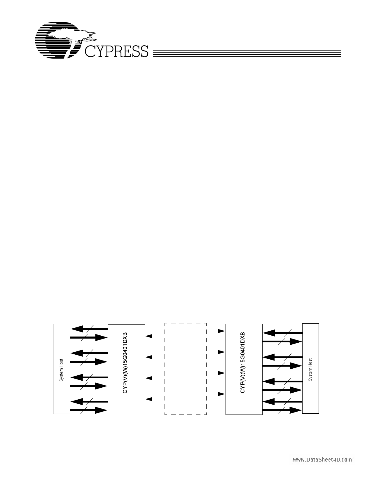
Functional Description
The CYP(V)15G0401DXB[1] Quad HOTLink II™ Transceiver
is a point-to-point or point-to-multipoint communications
building block allowing the transfer of data over high-speed
serial links (optical fiber, balanced, and unbalanced copper
transmission lines) at signaling speeds ranging from
195-to-1500 MBaud per serial link.
10
10
Serial Links
10
10
10
10
Serial Links
10
10
10
10
Serial Links
10
10
10
10
Serial Links
Backplane or
Cabled
Connections
10
10
Figure 1. HOTLink II System Connections
Note:
1. CYV15G0401DXB refers to SMPTE 259M and SMPTE 292M compliant devices. CYW15G0401DXB refers to OBSAI RP3 compliant devices (maximum
operating data rate is 1540 MBaud). CYP15G0401DXB refers to devices not compliant to SMPTE 259M and SMPTE 292M pathological test requirements and
also OBSAI RP3 operating datarate of 1536 MBaud. CYP(V)(W)15G0401DXB refers to all three devices.
Cypress Semiconductor Corporation • 3901 North First Street • San Jose, CA 95134 • 408-943-2600
Document #: 38-02002 Rev. *L
Revised March 30, 2005
1 page 
Receive Path Block Diagram
RXLE
BOE[7:0]
RX PLL Enable
Latch
Parity Control
Character-Rate Clock
SDASEL
LPEN
INSELA
INA1+
INA1–
www.DataSheet4U.com INA2+
INA2–
TXLBA
Receive
Signal
Monitor
Clock &
Data
Recovery
PLL
INSELB
INB1+
INB1–
INB2+
INB2–
TXLBB
Receive
Signal
Monitor
Clock &
Data
Recovery
PLL
INSELC
INC1+
INC1–
INC2+
INC2–
TXLBC
Receive
Signal
Monitor
Clock &
Data
Recovery
PLL
INSELD
IND1+
IND1–
IND2+
IND2–
TXLBD
RBIST[D:A]
FRAMCHAR
RXRATE
RFEN
RFMODE
RXCKSEL
DECMODE
RXMODE[1:0]
2
Receive
Signal
Monitor
Clock &
Data
Recovery
PLL
Document #: 38-02002 Rev. *L
CYP15G0401DXB
CYV15G0401DXB
CYW15G0401DXB
JTAG
Boundary
Scan
Controller
= Internal Signal
TRSTZ
TMS
TCLK
TDI
TDO
LFIA
8 RXDA[7:0]
RXOPA
3 RXSTA[2:0]
Clock
Select
÷2
RXCLKA+
RXCLKA–
LFIB
8 RXDB[7:0]
RXOPB
3 RXSTB[2:0]
Clock
Select
÷2
RXCLKB+
RXCLKB–
LFIC
8 RXDC[7:0]
RXOPC
3 RXSTC[2:0]
Clock
Select
÷2
RXCLKC+
RXCLKC–
LFID
8 RXDD[7:0]
RXOPD
3 RXSTD[2:0]
Clock
Select
÷2
RXCLKD+
RXCLKD–
Bonding
Control
2
BONDST
BOND_ALL
BOND_INH
MASTER
Page 5 of 53
5 Page 
CYP15G0401DXB
CYV15G0401DXB
CYW15G0401DXB
Pin Descriptions (continued)
CYP(V)(W)15G0401DXB Quad HOTLink II Transceiver
Pin Name
RXCLKA±
RXCLKB±
RXCLKC±
RXCLKD±
I/O Characteristics
Three-state, LVTTL
Output clock or static
control input
www.DataSheet4U.com
RXCKSEL
Three-level Select [5],
static control input
Signal Description
Receive Character Clock Output or Clock Select Input. When configured such that
all output data paths are clocked by the recovered clock (RXCKSEL = MID), these
true and complement clocks are the receive interface clocks which are used to control
timing of output data (RXDx[7:0], RXSTx[2:0] and RXOPx). These clocks are output
continuously at either the dual-character rate (1/20th the serial bit-rate) or character
rate (1/10th the serial bit-rate) of the data being received, as selected by RXRATE.
When configured such that all output data paths are clocked by REFCLK instead of a
recovered clock (RXCKSEL = LOW), the RXCLKA± and RXCLKC± output drivers
present a buffered and delayed form of REFCLK. RXCLKA± and RXCLKC± are
buffered forms of REFCLK that are slightly different in phase. This phase difference
allows the user to select the optimal setup/hold timing for their specific interface.
When RXCKSEL = LOW and quad channel bonding is enabled, RXCLKB+ and
RXCLKD+ are static control inputs used to select the master channel for bonding and
status control.
When RXCKSEL = HIGH and quad-channel bonding is enabled, one of the recovered
clocks from channels A, B, C or D can be selected to clock the bonded output data.
The selection of the recovered clock is made by RXCLKB+ and RXCLKD+ which act
as static control inputs in this mode. Both RXCLKA± and RXCLKC± output buffered
forms of the recovered clock selected from receive channel A, B, C, or D. See Table 15
for details.
When RXCKSEL = HIGH and dual-channel bonding is enabled, one of the recovered
clocks from channels A or B is selected to present bonded data from channels A and
B, and one of the recovered clocks from channels C or D is selected to present bonded
data from channels C and D. RXCLKA± output the recovered clock from either receive
channel A or receive channel B as selected by RXCLKB+ to clock the bonded output
data from channels A and B, and RXCLKC± output the recovered clock from either
receive channel C or receive channel D as selected by RXCLKD+ to the clock the
bonded output data from channels C and D. See Table 16 for details.
Receive Clock Mode. Selects the receive clock source used to transfer data to the
Output Registers.
When LOW, all four Output Registers are clocked by REFCLK. RXCLKB± and
RXCLKD± outputs are disabled (High-Z), and RXCLKA± and RXCLKC± present
buffered and delayed forms of REFCLK. This clocking mode is required for channel
bonding across multiple devices.
When MID, each RXCLKx± output follows the recovered clock for the respective
channel, as selected by RXRATE. When the 10B/8B Decoder and Elasticity Buffer are
bypassed (DECMODE = LOW), RXCKSEL must be MID.
When HIGH and channel bonding is enabled in dual-channel mode (RX modes 3 and
5), RXCLKA± outputs the recovered clock from either receive channel A or B as
selected by RXCLKB+, and RXCLKC± outputs the recovered clock from either receive
channel C or D as selected by RXCLKD+. These output clocks may operate at the
character-rate or half the character-rate as selected by RXRATE.
When HIGH and channel bonding is enabled in quad channel mode (RX modes 6 and
8), or if the receive channels are operated in independent mode (RX modes 0 and 2),
RXCLKA± and RXCLKC± output the recovered clock from receive channel A, B, C,
or D, as selected by RXCLKB+ and RXCLKD+. This output clock may operate at the
character-rate or half the character-rate as selected by RXRATE.
Document #: 38-02002 Rev. *L
Page 11 of 53
11 Page | ||
| Páginas | Total 30 Páginas | |
| PDF Descargar | [ Datasheet CYW15G0401DXB.PDF ] | |
Hoja de datos destacado
| Número de pieza | Descripción | Fabricantes |
| CYW15G0401DXB | Transceiver | Cypress Semiconductor |
| Número de pieza | Descripción | Fabricantes |
| SLA6805M | High Voltage 3 phase Motor Driver IC. |
Sanken |
| SDC1742 | 12- and 14-Bit Hybrid Synchro / Resolver-to-Digital Converters. |
Analog Devices |
|
DataSheet.es es una pagina web que funciona como un repositorio de manuales o hoja de datos de muchos de los productos más populares, |
| DataSheet.es | 2020 | Privacy Policy | Contacto | Buscar |