|
|
|
PDF AAT1275 Data sheet ( Hoja de datos )
| Número de pieza | AAT1275 | |
| Descripción | Boost Converter | |
| Fabricantes | AAT | |
| Logotipo | ||
Hay una vista previa y un enlace de descarga de AAT1275 (archivo pdf) en la parte inferior de esta página. Total 19 Páginas | ||
|
No Preview Available !
www.DataSheet4U.com
AAT1275
Boost Converter with USB Power Switch
General Description
Features
SwitchReg™
The AAT1275 SwitchReg is a 2MHz, 500mA syn-
chronous boost converter with an integrated current-
limiting load switch controlled output. The AAT1275
operates from a single-cell Lithium-ion/ polymer bat-
tery source and provides a regulated 5V, current
limit controlled output to support USB port VBUS
applications in portable consumer electronic prod-
ucts. The AAT1275 can support both USB 2.0 host
port and USB on-the-go operation, as well as gen-
eral purpose applications where a 5V supply with a
user programmable current limit is needed.
The high efficiency boost converter section of the
AAT1275 is typically set for a 5V output and can
deliver up to 500mA load current to support USB
VBUS operation from an input supply as low as
2.7V. The high boost converter switching frequen-
cy (up to 2.0MHz) provides fast load transient and
allows the use of small external components. Fully
integrated control circuitry simplifies system design
and reduces total solution size.
The integrated, programmable current limiting load
switch provides USB port protection for portable
devices allowing the AAT1275 to supply a 5V USB
VBUS up to 500mA. The load switch provides an
active low fault flag to alert the system in the event
of an over-current condition applied to the
AAT1275 output.
The AAT1275 is available in the Pb-free, space-
saving 12-pin TSOPJW and 16-pin TDFN34 pack-
ages and is rated over the -40°C to +85°C operat-
ing temperature range.
• High Frequency Boost With 5V / 500mA
Output Capability From a Single-Cell Lithium-
Ion/Polymer Battery
• Input Voltage Range: 2.7V to 5V
• VOUT1 Adjustable or Fixed (5V)
• >90% Efficiency
• Up to 2MHz Switching Frequency
• True Load Disconnect
• Load Switch With Programmable Current Limit
• Over-Temperature, Over-Current Protection
• Inrush Current Limit
• Fault Report
• Low Shutdown Current < 1µA Typical
• -40°C to +85°C Temperature Range
• TSOPJW-12 and TDFN34-16 Packages
Applications
• USB On-the-Go
• Cell Phones
• Digital Still Cameras
• PDAs and Portable Media Players
• Smart Phones
• Other Hand-Held Devices
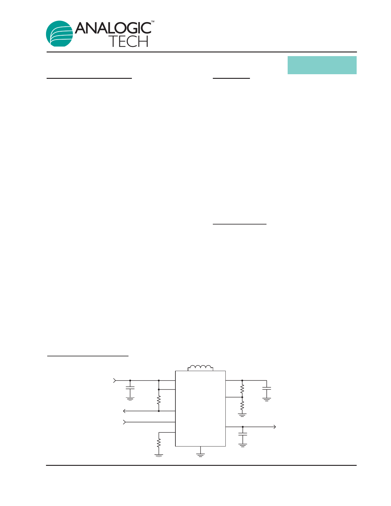
Typical Application
VIN
Fault
Enable
CIN
4.7µF
10k
RSET
L1 2.2µH
LIN
IN
SW
OUT1
VCC
FB
AAT1275
FLT
EN
SET
OUT2
GND
RFB1
432k
RFB2
59k
COUT1
4.7µF
COUT2
1µF
VBUS Output
1275.2007.01.1.3
1
1 page 
AAT1275
Boost Converter with USB Power Switch
Typical Characteristics
Efficiency vs. Load
100
80
60
40
20
0
0.1
VIN = 2.7V
VIN = 4.2V
VIN = 3.6V
1 10 100
Output Current (mA)
1000
1.5
1.0
0.5
0.0
-0.5
-1.0
-1.5
0.1
DC Regulation
(VOUT = 5.0V)
VIN = 4.2V
VIN = 2.7V VIN = 3.6V
1 10 100
Output Current (mA)
1000
Line Regulation
(IOUT = 300mA)
4.960
4.958
4.956
4.954
4.952
4.950
4.948
4.946
4.944
4.942
4.940
3.6 3.7 3.8 3.9 4.0 4.1 4.2
Input Voltage (V)
Output Voltage vs. Temperature
(VIN = 3.6V; 50Ω Load)
0.1
0.0
-0.1
-0.2
-0.3
-0.4
-0.5
-0.6
-0.7
-50
-25
0
25 50 75
Temperature (°C)
100
No Load Current vs. Supply Voltage
140
120
85°C
100
80
60
-40°C
25°C
40
20
0
2.7 2.9 3.2 3.4 3.6 3.9 4.1 4.3 4.5 4.8 5.0
Supply Voltage (V)
No Load Current vs. Temperature
(VIN = 3.6V; VOUT = 5.0V)
140
120
100
80
60
40
20
0
-50
0
50 100
Temperature (°C)
150
1275.2007.01.1.3
5
5 Page 
AAT1275
Boost Converter with USB Power Switch
Selecting the Boost Inductor
The AAT1275 boost controller utilizes hysteretic
control and the switching frequency varies with out-
put load and input voltage. The value of the induc-
tor determines the maximum switching frequency
of the boost converter. Increasing output induc-
tance decreases the switching frequency, resulting
in higher peak currents and increased output volt-
age ripple. To maintain the 2MHz switching fre-
quency and stable operation, an output inductor
sized from 1.5µH to 2.7µH is recommended.
Manufacturer's specifications list both the inductor
DC current rating, which is a thermal limitation, and
peak inductor current rating, which is a function of
the saturation characteristics.
Measure the inductor current at full load and high
ambient temperature to ensure that the inductor
does not saturate or exhibit excessive temperature
rise. Select the output inductor (L) to avoid satura-
tion at the minimum input voltage and maximum
load. The RMS current flowing through the boost
inductor is equal to the DC plus AC ripple compo-
nents. The maximum inductor RMS current occurs
at the minimum input voltage and the maximum
load. Use the following equations to calculate the
maximum peak and RMS current:
DMAX
= VO
-
VIN(MIN)
VO
IPP
=
VIN(MIN) · D
L · FS
IP
=
IO
1-D
IPK = IP +
IPP
2
IV = IP - IPP
IRMS =
IPK2 + IPK · IV + IV2
3
PLOSS(INDUCTOR) = I2RMS · DCR
At light load and low output voltage, the controller
reduces the operating frequency to maintain maxi-
mum efficiency. As a result, further reduction in out-
put load does not reduce the peak current. The
minimum peak current ranges from 0.5A to 0.75A.
Compare the RMS current values with the manu-
facturer's temperature rise, or thermal derating
guidelines. For a given inductor type, smaller
inductor size leads to an increase in DCR winding
resistance and, in most cases, increased thermal
impedance. Winding resistance degrades boost
converter efficiency and increases the inductor's
operating temperature.
Shielded inductors provide decreased EMI and
may be required in noise sensitive applications.
Unshielded chip inductors provide significant space
savings at a reduced cost compared to shielded
inductors. In general, chip-type inductors have
increased winding resistance (DCR) when com-
pared to shielded, wound varieties.
Selecting the Step-Up Converter
Capacitors
The high output ripple inherent in the boost con-
verter necessitates low impedance output filtering.
Multi-layer ceramic (MLC) capacitors provide small
size, adequate capacitance, with low parasitic
equivalent series resistance (ESR) and equivalent
series inductance (ESL). This makes them well
suited for use with the AAT1275. MLC capacitors of
type X7R or X5R ensure good capacitance stabili-
ty over the full operating range. MLC capacitors
exhibit significant capacitance reduction with an
applied DC voltage. Output ripple measurements
can confirm that the capacitance used meets the
specific ripple requirements. Voltage derating mini-
1275.2007.01.1.3
11
11 Page | ||
| Páginas | Total 19 Páginas | |
| PDF Descargar | [ Datasheet AAT1275.PDF ] | |
Hoja de datos destacado
| Número de pieza | Descripción | Fabricantes |
| AAT1270 | 1A Step-Up Current Regulator | AAT |
| AAT1274 | 1.5A Single Flash LED Driver IC | Skyworks Solutions |
| AAT1275 | Boost Converter | AAT |
| AAT1276 | Boost Converter | Advanced Analogic Technologies |
| Número de pieza | Descripción | Fabricantes |
| SLA6805M | High Voltage 3 phase Motor Driver IC. |
Sanken |
| SDC1742 | 12- and 14-Bit Hybrid Synchro / Resolver-to-Digital Converters. |
Analog Devices |
|
DataSheet.es es una pagina web que funciona como un repositorio de manuales o hoja de datos de muchos de los productos más populares, |
| DataSheet.es | 2020 | Privacy Policy | Contacto | Buscar |