|
|
|
PDF ISL6753 Data sheet ( Hoja de datos )
| Número de pieza | ISL6753 | |
| Descripción | ZVS Full-Bridge PWM Controller | |
| Fabricantes | Intersil Corporation | |
| Logotipo | ||
Hay una vista previa y un enlace de descarga de ISL6753 (archivo pdf) en la parte inferior de esta página. Total 15 Páginas | ||
|
No Preview Available !
®
Data Sheet
April 4, 2006
ISL6753
FN9182.2
ZVS Full-Bridge PWM Controller
The ISL6753 is a high-performance, low-pin-count
alternative, zero-voltage switching (ZVS) full-bridge PWM
controller. Like the ISL6551, it achieves ZVS operation by
driving the upper bridge FETs at a fixed 50% duty cycle while
the lower bridge FETS are trailing-edge modulated with
adjustable resonant switching delays. Compared to the more
familiar phase-shifted control method, this algorithm offers
equivalent efficiency and improved overcurrent and light-
load performance with less complexity in a lower pin count
package.
This advanced BiCMOS design features low operating
current, adjustable oscillator frequency up to 2MHz,
adjustable soft-start, internal over temperature protection,
precision deadtime and resonant delay control, and short
propagation delays. Additionally, Multi-Pulse Suppression
ensures alternating output pulses at low duty cycles where
pulse skipping may occur.
Ordering Information
PART
NUMBER
PART
TEMP.
PKG.
MARKING RANGE (°C) PACKAGE DWG. #
ISL6753AAZA ISL6753AAZ -40 to 105 16 Ld QSOP M16.15A
(See Note)
(Pb-free)
Add -T suffix to part number for tape and reel packaging
NOTE: Intersil Pb-free plus anneal products employ special Pb-free
material sets; molding compounds/die attach materials and 100%
matte tin plate termination finish, which are RoHS compliant and
compatible with both SnPb and Pb-free soldering operations. Intersil
Pb-free products are MSL classified at Pb-free peak reflow
temperatures that meet or exceed the Pb-free requirements of
IPC/JEDEC J STD-020.
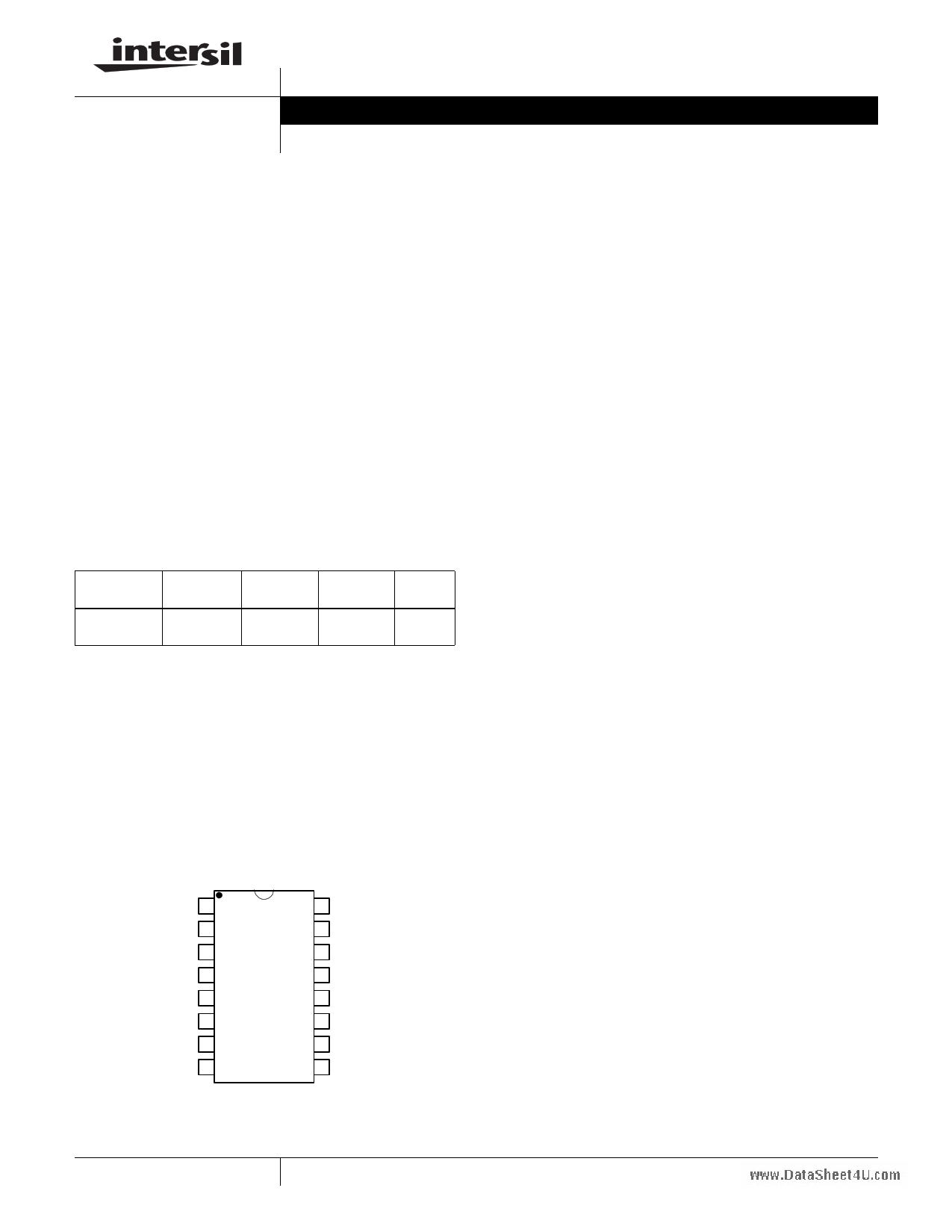
Pinout
ISL6753 (QSOP)
TOP VIEW
VERR 1
CTBUF 2
RTD 3
RESDEL 4
CT 5
FB 6
RAMP 7
CS 8
16 VREF
15 SS
14 VDD
13 OUTLL
12 OUTLR
11 OUTUL
10 OUTUR
9 GND
Features
• Adjustable Resonant Delay for ZVS Operation
• Voltage- or Current-Mode Operation
• 3% Current Limit Threshold
• 175µA Startup Current
• Supply UVLO
• Adjustable Deadtime Control
• Adjustable Soft-Start
• Adjustable Oscillator Frequency Up to 2MHz
• Tight Tolerance Error Amplifier Reference Over Line,
Load, and Temperature
• 5MHz GBWP Error Amplifier
• Adjustable Cycle-by-Cycle Peak Current Limit
• Fast Current Sense to Output Delay
• 70ns Leading Edge Blanking
• Multi-Pulse Suppression
• Buffered Oscillator Sawtooth Output
• Internal Over Temperature Protection
• Pb-Free Plus Anneal Available and ELV, WEEE,
RoHS Compliant
Applications
• ZVS Full-Bridge Converters
• Telecom and Datacom Power
• Wireless Base Station Power
• File Server Power
• Industrial Power Systems
1
CAUTION: These devices are sensitive to electrostatic discharge; follow proper IC Handling Procedures.
1-888-INTERSIL or 1-888-468-3774 | Intersil (and design) is a registered trademark of Intersil Americas Inc.
Copyright Intersil Americas Inc. 2005, 2006. All Rights Reserved
All other trademarks mentioned are the property of their respective owners.
1 page 
ISL6753
Electrical Specifications
Recommended operating conditions unless otherwise noted. Refer to Block Diagram and Typical Application
schematic. 9V < VDD < 20V, RTD = 10.0kΩ, CT = 470pF, TA = -40°C to 105°C (Note 3), Typical values are at
TA = 25°C (Continued)
PARAMETER
TEST CONDITIONS
MIN
TYP
MAX
UNITS
Bias Current
Clamp Voltage
VRAMP = 0.3V
(Note 4)
-5.0 - -2.0 µA
6.5 - 8.0 V
PULSE WIDTH MODULATOR
Minimum Duty Cycle
VERR < 0.6V
- - 0%
Maximum Duty Cycle (per half-cycle)
VERR = 4.20V, VRAMP = 0V,
VCS = 0V (Note 5)
RTD = 2.00kΩ, CT = 220pF
- 94 - %
- 97 - %
Zero Duty Cycle VERR Voltage
VERR to PWM Comparator Input Offset
VERR to PWM Comparator Input Gain
Common Mode (CM) Input Range
ERROR AMPLIFIER
Input Common Mode (CM) Range
GBWP
VERR VOL
VERR VOH
VERR Pull-Up Current Source
EA Reference
EA Reference + EA Input Offset Voltage
OSCILLATOR
Frequency Accuracy, Overall
Frequency Variation with VDD
Temperature Stability
Charge Current
Discharge Current Gain
CT Valley Voltage
CT Peak Voltage
CT Pk-Pk Voltage
RTD Voltage
RESDEL Voltage Range
CTBUF Gain (VCTBUFp-p/VCTp-p)
CTBUF Offset from GND
CTBUF VOH
RTD = 2.00kΩ, CT = 470pF
TA = 25°C
(Note 4)
-
0.85
0.7
0.31
0
(Note 4)
(Note 4)
ILOAD = 2mA
ILOAD = 0mA
VERR = 2.5V
TA = 25°C
0
5
-
4.20
0.8
0.594
0.590
(Note 4)
TA = 25°C, (F20V- - F10V)/F10V
VDD = 10V, |F-40°C - F0°C|/F0°C
|F0°C - F105°C|/F25°C
(Note 4)
TA = 25°C
Static Threshold
Static Threshold
Static Value
VCT = 0.8V, 2.6V
VCT = 0.8V
∆V(ILOAD = 0mA, ILOAD = -2mA),
VCT = 2.6V
165
-10
-
-
-
-193
19
0.75
2.75
1.92
1.97
0
1.95
0.34
-
99
-
0.8
0.33
-
-
-
-
-
1.0
0.600
0.600
183
-
0.3
4.5
1.5
-200
20
0.80
2.80
2.00
2.00
-
2.0
0.40
-
-
1.20
0.9
0.35
VSS
VREF
-
0.4
-
1.3
0.606
0.612
201
+10
1.7
-
-
-207
23
0.88
2.88
2.05
2.03
2
2.05
0.44
0.10
%
V
V
V/V
V
V
MHz
V
V
mA
V
V
kHz
%
%
%
%
µA
µA/µA
V
V
V
V
V
V/V
V
V
5 FN9182.2
April 4, 2006
5 Page 
ISL6753
For simplicity, idealized components have been used for this
discussion, but the effect of magnetizing inductance must be
considered when determining the amount of external ramp
to add. Magnetizing inductance provides a degree of slope
compensation to the current feedback signal and reduces
the amount of external ramp required. The magnetizing
inductance adds primary current in excess of what is
reflected from the inductor current in the secondary.
∆IP
=
-V----I--N-----⋅---D-----T----S----W---
Lm
A
(EQ. 19)
where VIN is the input voltage that corresponds to the duty
cycle D and Lm is the primary magnetizing inductance. The
effect of the magnetizing current at the current sense
resistor, RCS, is
∆VCS
=
∆-----I--P-----⋅---R----C----S--
NCT
V
(EQ. 20)
If ∆VCS is greater than or equal to Ve, then no additional
slope compensation is needed and RCS becomes
RCS
=
--------------------------------------------------------------N----C----T---------------------------------------------------------------
N-----S--
NP
⋅
I O
+
D-----T----S----W---
2LO
⋅
VI
N
⋅
N-----S--
NP
–
VO
+
V-----I--N-----⋅---D-----T----S---W----
Lm
(EQ. 21)
If ∆VCS is less than Ve, then Equation 18 is still valid for the
value of RCS, but the amount of slope compensation added
by the external ramp must be reduced by ∆VCS.
Adding slope compensation is accomplished in the ISL6753
using the CTBUF signal. CTBUF is an amplified
representation of the sawtooth signal that appears on the CT
pin. It is offset from ground by 0.4V and is 2x the peak-to-
peak amplitude of CT (0.4 - 4.4V). A typical application sums
this signal with the current sense feedback and applies the
result to the CS pin as shown in Figure 7.
R9
R6
RCS
1
2 CTBUF
3
4
ISL6753
5
6
7
8 CS
C4
FIGURE 7. ADDING SLOPE COMPENSATION
Assuming the designer has selected values for the RC filter
placed on the CS pin, the value of R9 required to add the
appropriate external ramp can be found by superposition.
Ve – ∆VCS
=
-(--D-----(--V----C-----T---B----U----F-----–-----0---.--4---)----+-----0---.--4---)----⋅---R-----6-
R6 + R9
V
(EQ. 22)
Rearranging to solve for R9 yields
R9 = (---D-----(--V----C-----T---B----U----F-----–-----0---.--4---)----–----V-----e----+-----∆----V----C----S-----+-----0----.-4----)----⋅---R----6--
Ve – ∆VCS
Ω
(EQ. 23)
The value of RCS determined in Equation 18 must be
rescaled so that the current sense signal presented at the
CS pin is that predicted by Equation 16. The divider created
by R6 and R9 makes this necessary.
R′CS
=
R-----6-----+-----R-----9--
R9
⋅
RCS
(EQ. 24)
Example:
VIN = 280V
VO = 12V
LO = 2.0µH
Np/Ns = 20
Lm = 2mH
IO = 55A
Oscillator Frequency, Fsw = 400kHz
Duty Cycle, D = 85.7%
NCT = 50
R6 = 499Ω
Solve for the current sense resistor, RCS, using Equation 18.
RCS = 15.1Ω.
Determine the amount of voltage, Ve, that must be added to
the current feedback signal using Equation 15.
Ve = 153mV
Next, determine the effect of the magnetizing current from
Equation 20.
∆VCS = 91mV
Using Equation 23, solve for the summing resistor, R9, from
CTBUF to CS.
R9 = 30.1kΩ
Determine the new value of RCS, R’CS, using Equation 24.
R’CS = 15.4Ω
The above discussion determines the minimum external
ramp that is required. Additional slope compensation may be
considered for design margin.
11 FN9182.2
April 4, 2006
11 Page | ||
| Páginas | Total 15 Páginas | |
| PDF Descargar | [ Datasheet ISL6753.PDF ] | |
Hoja de datos destacado
| Número de pieza | Descripción | Fabricantes |
| ISL6752 | ZVS Full-Bridge Current-Mode PWM | Intersil Corporation |
| ISL6753 | ZVS Full-Bridge PWM Controller | Intersil Corporation |
| ISL6754 | ZVS Full-Bridge PWM Controller | Intersil |
| ISL6755 | ZVS Full-Bridge PWM Controller | Intersil |
| Número de pieza | Descripción | Fabricantes |
| SLA6805M | High Voltage 3 phase Motor Driver IC. |
Sanken |
| SDC1742 | 12- and 14-Bit Hybrid Synchro / Resolver-to-Digital Converters. |
Analog Devices |
|
DataSheet.es es una pagina web que funciona como un repositorio de manuales o hoja de datos de muchos de los productos más populares, |
| DataSheet.es | 2020 | Privacy Policy | Contacto | Buscar |