|
|
|
PDF RF3S49092SM Data sheet ( Hoja de datos )
| Número de pieza | RF3S49092SM | |
| Descripción | Complementary Power MOSFET | |
| Fabricantes | Fairchild Semiconductor | |
| Logotipo | ||
Hay una vista previa y un enlace de descarga de RF3S49092SM (archivo pdf) en la parte inferior de esta página. Total 14 Páginas | ||
|
No Preview Available !
Data Sheet
RF3S49092SM
September 2004
20A/10A, 12V, 0.060/0.140 Ohm, Logic
Level, Complementary Power MOSFET
These complementary power MOSFETs are manufactured
using an advanced MegaFET process. This process, which
uses feature sizes approaching those of LSI integrated
circuits, gives optimum utilization of silicon, resulting in
outstanding performance. It is designed for use in
applications such as switching regulators, switching
converters, motor drivers, relay drivers, and low voltage bus
switches. This product achieves full rated conduction at a
gate bias in the 3V to 5V range, thereby facilitating true
on-off power control directly from logic level (5V) integrated
circuits.
Formerly developmental type TA49092.
Ordering Information
PART NUMBER
PACKAGE
BRAND
RF3S49092SM
MO-169AB
F3S49092
NOTE: When ordering, use the entire part number. For ordering the
MO-169AB in tape and reel, add the suffix 9A to the part number, i.e.,
RF3S49092SM9A.
Features
• 20A, 12V (N-Channel)
10A, 12V (P-Channel)
• rDS(ON) = 0.060Ω (N-Channel)
rDS(ON) = 0.140Ω (P-Channel)
• Temperature Compensating PSPICE® Model
• On-Resistance vs Gate Drive Voltage Curves
• Peak Current vs Pulse Width Curve
• UIS Rating Curve
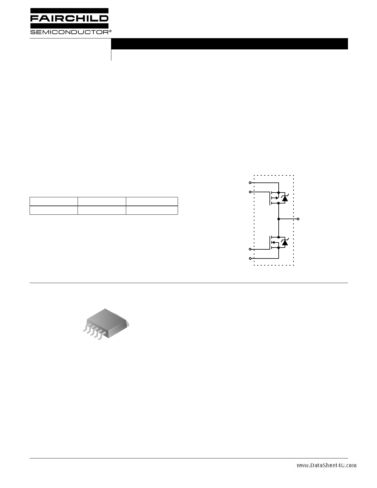
Symbol
S2
G2
D1
G1
S1
Packaging
JEDEC MO-169AB
G2
S2 D G1
S1
©2004 Fairchild Semiconductor Corporation
RF3S49092SM Rev. C
1 page 
RF3S49092SM
Typical Performance Curves (N-Channel) (Continued)
50
25oC
VDD = 6V
175oC
40
-55oC
30
20
10
PULSE DURATION = 80µs
DUTY CYCLE = 0.5% MAX
0
01234567
VGS, GATE TO SOURCE VOLTAGE (V)
FIGURE 8. TRANSFER CHARACTERISTICS
140
VDD = 6V, ID = 20A, RL = 0.24Ω
120
100
80
60
tr
tD(OFF)
tf
40
20
t D(ON)
0
0 10 20 30 40 50
RGS, GATE TO SOURCE RESISTANCE (Ω)
FIGURE 10. SWITCHING TIME vs GATE RESISTANCE
200
ID = 5A
150
ID = 10A
100
ID = 20A
50
PULSE DURATION = 80µs
DUTY CYCLE = 0.5% MAX
0
024
6
8
VGS, GATE TO SOURCE VOLTAGE (V)
10
FIGURE 9. DRAIN TO SOURCE ON RESISTANCE vs GATE
VOLTAGE AND DRAIN CURRENT
1.6
PULSE DURATION = 80µs, VGS = 5V, ID = 20A
DUTY CYCLE = 0.5% MAX
1.4
1.2
1.0
0.8
0.6
-80
-40 0 40 80 120 160
TJ, JUNCTION TEMPERATURE (oC)
200
FIGURE 11. NORMALIZED DRAIN TO SOURCE ON
RESISTANCE vs JUNCTION TEMPERATURE
1.2 1.2
VGS = VDS, ID = 250µA
ID = 250µA
1.0 1.1
0.8 1.0
0.6
-80
-40 0
40 80 120 160
TJ, JUNCTION TEMPERATURE (oC)
200
FIGURE 12. NORMALIZED GATE THRESHOLD VOLTAGE vs
JUNCTION TEMPERATURE
©2004 Fairchild Semiconductor Corporation
0.9
-80
-40 0 40 80 120 160
TJ, JUNCTION TEMPERATURE (oC)
200
FIGURE 13. NORMALIZED DRAIN TO SOURCE BREAKDOWN
VOLTAGE vs JUNCTION TEMPERATURE
RF3S49092SM Rev. C
5 Page 
RF3S49092SM
Soldering Precautions
The soldering process creates a considerable thermal stress
on any semiconductor component. The melting temperature
of solder is higher than the maximum rated temperature of
the device. The amount of time the device is heated to a high
temperature should be minimized to assure device reliability.
Therefore, the following precautions should always be
observed in order to minimize the thermal stress to which the
devices are subjected.
1. Always preheat the device.
2. The delta temperature between the preheat and soldering
should always be less than 100oC. Failure to preheat the
device can result in excessive thermal stress which can
damage the device.
3. The maximum temperature gradient should be less than
5oC per second when changing from preheating to
soldering.
4. The peak temperature in the soldering process should be
at least 30oC higher than the melting point of the solder
chosen.
5. The maximum soldering temperature and time must not
exceed 260oC for 10 seconds on the leads and case of
the device.
6. After soldering is complete, the device should be allowed
to cool naturally for at least three minutes, as forced cool-
ing will increase the temperature gradient and may result
in latent failure due to mechanical stress.
7. During cooling, mechanical stress or shock should be
avoided.
©2004 Fairchild Semiconductor Corporation
RF3S49092SM Rev. C
11 Page | ||
| Páginas | Total 14 Páginas | |
| PDF Descargar | [ Datasheet RF3S49092SM.PDF ] | |
Hoja de datos destacado
| Número de pieza | Descripción | Fabricantes |
| RF3S49092SM | 20A/10A/ 12V/ 0.060/0.140 Ohm/ Logic Level/ Complementary Power MOSFET | Intersil Corporation |
| RF3S49092SM | Complementary Power MOSFET | Fairchild Semiconductor |
| Número de pieza | Descripción | Fabricantes |
| SLA6805M | High Voltage 3 phase Motor Driver IC. |
Sanken |
| SDC1742 | 12- and 14-Bit Hybrid Synchro / Resolver-to-Digital Converters. |
Analog Devices |
|
DataSheet.es es una pagina web que funciona como un repositorio de manuales o hoja de datos de muchos de los productos más populares, |
| DataSheet.es | 2020 | Privacy Policy | Contacto | Buscar |