|
|
PDF HY5V62CF Data sheet ( Hoja de datos )
| Número de pieza | HY5V62CF | |
| Descripción | 4 Banks X 512K X 32Bit Synchronous DRAM | |
| Fabricantes | Hynix Semiconductor | |
| Logotipo | ||
Hay una vista previa y un enlace de descarga de HY5V62CF (archivo pdf) en la parte inferior de esta página. Total 11 Páginas | ||
|
No Preview Available !
www.DataSheet4U.com
HY5V62CF
4 Banks x 512K x 32Bit Synchronous DRAM
DESCRIPTION
The Hynix HY5V62C is a 67,108,864-bit CMOS Synchronous DRAM, ideally suited for the memory applications which
require wide data I/O and high bandwidth. HY5V62C is organized as 4banks of 524,288x32.
HY5V62C is offering fully synchronous operation referenced to a positive edge of the clock. All inputs and outputs are
synchronized with the rising edge of the clock input. The data paths are internally pipelined to achieve very high band-
width. All input and output voltage levels are compatible with LVTTL.
Programmable options include the length of pipeline (Read latency of 2 or 3), the number of consecutive read or write
cycles initiated by a single control command (Burst length of 1,2,4,8 or full page), and the burst count
sequence(sequential or interleave). A burst of read or write cycles in progress can be terminated by a burst terminate
command or can be interrupted and replaced by a new burst read or write command on any cycle. (This pipelined
design is not restricted by a `2N` rule.)
FEATURES
• JEDEC standard 3.3V power supply
• All device pins are compatible with LVTTL interface
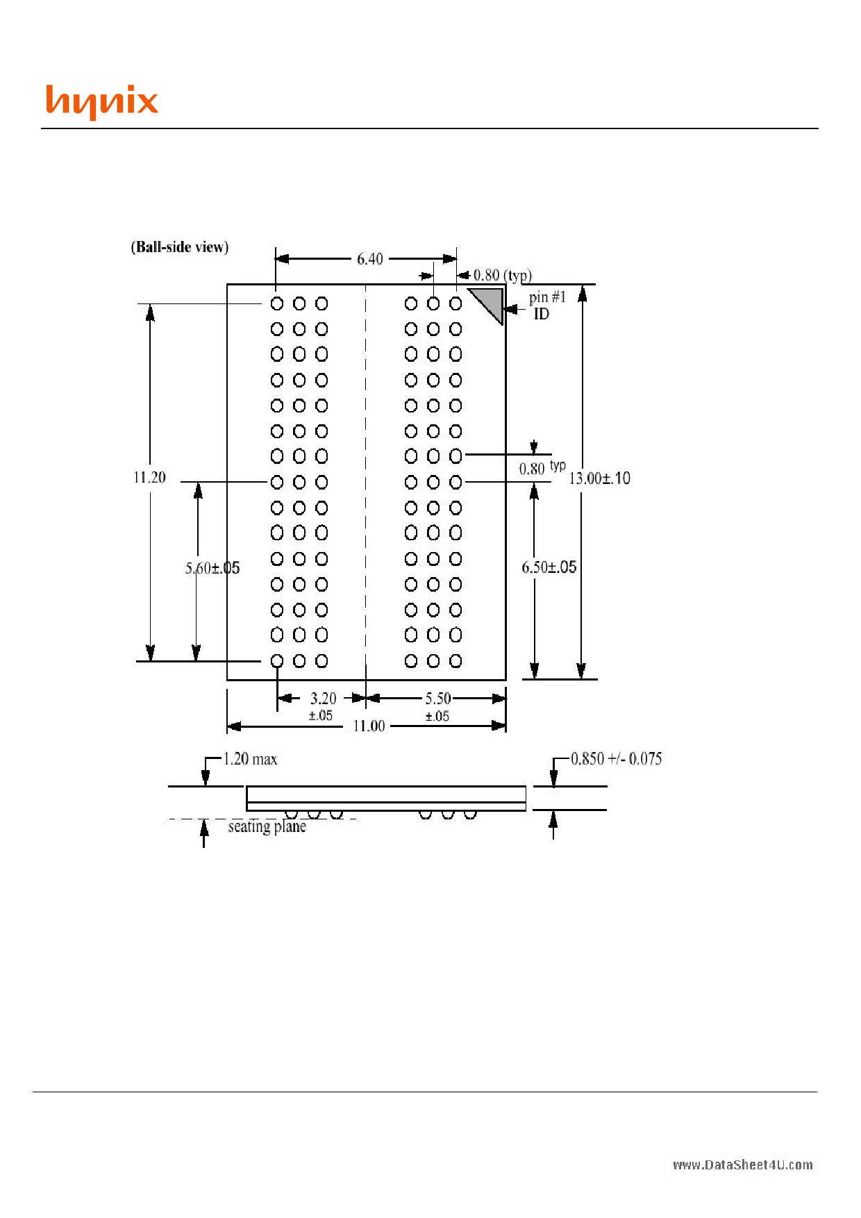
• 90Ball FBGA with 0.8mm of pin pitch
• All inputs and outputs referenced to positive edge of
system clock
• Data mask function by DQM0,1,2 and 3
• Internal four banks operation
• Auto refresh and self refresh
• 4096 refresh cycles / 64ms
• Programmable Burst Length and Burst Type
- 1, 2, 4, 8 or full page for Sequential Burst
- 1, 2, 4 or 8 for Interleave Burst
• Programmable CAS Latency ; 2, 3 Clocks
• Burst Read Single Write operation
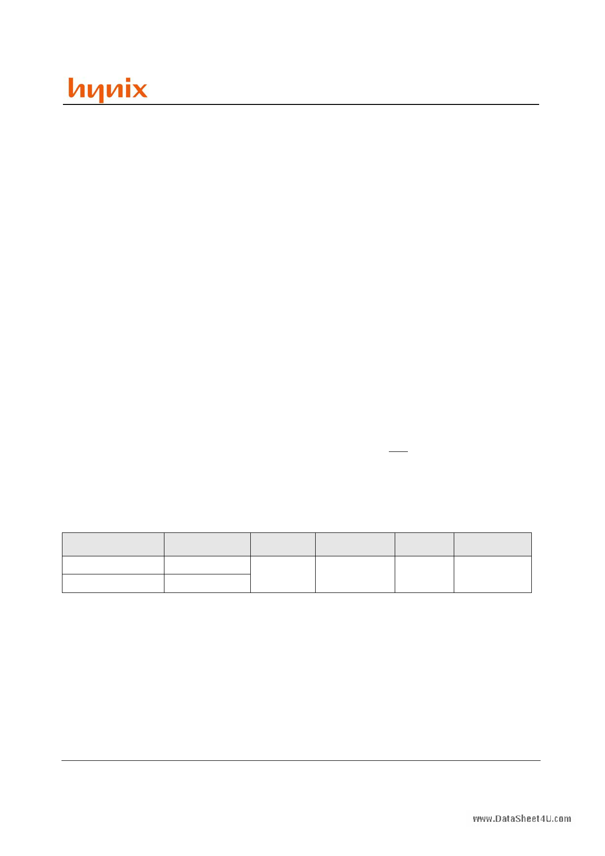
ORDERING INFORMATION
Part No.
HY5V62CF-7
HY5V62CF-S
Clock Frequency
143MHz
100MHz
Power
Normal
Organization Interface
4Banks x 512Kbits
x32
LVTTL
Package
90Ball FBGA
This document is a general product description and is subject to change without notice. Hynix Semiconductor Inc. does not assume
any responsibility for use of circuits described. No patent licenses are implied.
Rev. 0.4/Nov. 01
1 page 
www.DataSheet4U.com
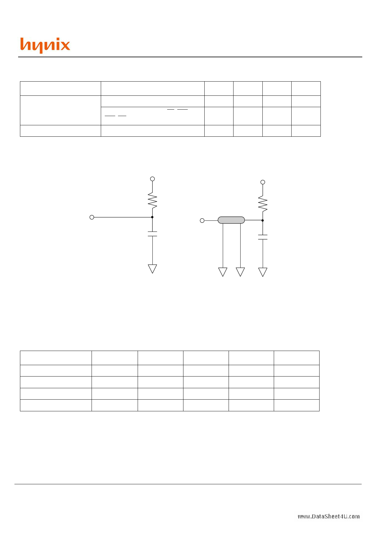
CAPACITANCE (TA=25°C, f=1MHz, VDD=3.3V)
Parameter
Input capacitance
Data input / output capacitance
Pin
CLK
A0 ~ A10, BA0, BA1, CKE, CS, RAS,
CAS, WE, DQM0~3
DQ0 ~ DQ31
OUTPUT LOAD CIRCUIT
Symbol
CI1
CI2
CI/O
Min
2.5
2.5
4
HY5V62CF
Max Unit
3.5 pF
3.8 pF
6.5 pF
Output
Vtt=1.4V
RT=500 Ω
30pF
Output
Z0 = 50Ω
Vtt=1.4V
RT=50 Ω
30pF
DC Output Load Circuit
AC Output Load Circuit
DC CHARACTERISTICS I (DC operating conditions unless otherwise noted)
Parameter
Symbol
Min.
Max
Unit
Note
Input leakage current
Output leakage current
Output high voltage
Output low voltage
ILI
ILO
VOH
VOL
-1 1 uA 1
-1 1 uA 2
2.4 -
V IOH = -2mA
- 0.4 V IOL = +2mA
Note :
1.VIN = 0 to 3.6V, All other pins are not under test = 0V
2.DOUT is disabled, VOUT=0 to 3.6V
Rev. 0.4/Nov. 01
6
5 Page 
www.DataSheet4U.com
PACKAGE INFORMATION
HY5V62CF
Rev. 0.4/Nov. 01
12
11 Page | ||
| Páginas | Total 11 Páginas | |
| PDF Descargar | [ Datasheet HY5V62CF.PDF ] | |
Hoja de datos destacado
| Número de pieza | Descripción | Fabricantes |
| HY5V62CF | 4 Banks X 512K X 32Bit Synchronous DRAM | Hynix Semiconductor |
| Número de pieza | Descripción | Fabricantes |
| SLA6805M | High Voltage 3 phase Motor Driver IC. |
Sanken |
| SDC1742 | 12- and 14-Bit Hybrid Synchro / Resolver-to-Digital Converters. |
Analog Devices |
|
DataSheet.es es una pagina web que funciona como un repositorio de manuales o hoja de datos de muchos de los productos más populares, |
| DataSheet.es | 2020 | Privacy Policy | Contacto | Buscar |
