|
|
|
PDF ICS9148-03 Data sheet ( Hoja de datos )
| Número de pieza | ICS9148-03 | |
| Descripción | Frequency Generator & Integrated Buffers | |
| Fabricantes | Integrated Circuit Systems | |
| Logotipo | ||
Hay una vista previa y un enlace de descarga de ICS9148-03 (archivo pdf) en la parte inferior de esta página. Total 12 Páginas | ||
|
No Preview Available !
Integrated
Circuit
Systems, Inc.
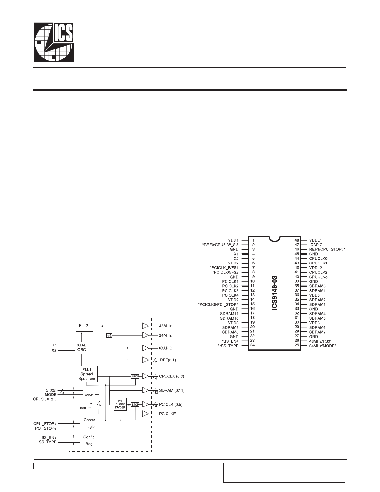
ICS9148 - 03
Frequency Generator & Integrated Buffers for PENTIUM/ProTM
General Description
The ICS9148-03 generates all clocks required for high
speed RISC or CISC microprocessor systems such as Intel
PentiumPro or Cyrix. Eight different reference frequency
multiplying factors are externally selectable with smooth
frequency transitions.
Features include four CPU, seven PCI and Twelve SDRAM
clocks. Two reference outputs are available equal to the
crystal frequency. Plus the IOAPIC output powered by
VDDL1. One 48 MHz for USB, and one 24 MHz clock for
Super IO. Spread Spectrum built in - ±1.5% modulation to
reduce the EMI. Rise time adjustment for VDD at 3.3V or
2.5V CPU. Additionally, the device meets the Pentium
power-up stabilization, which requires that CPU and PCI
clocks be stable within 2ms after power-up. It is not
recommended to use I/O dual function pin for the slots
(ISA, PCI, CPU, DIMM). The add on card might have a pull up
or pull down.
Features
3.3V outputs: SDRAM, PCI, REF, 48/24MHz.
2.5V or 3.3V outputs: CPU, IOAPIC
20 ohm CPU clock output impedance
20 ohm PCI clock output impedance
Skew from CPU (earlier) to PCI clock - 1 to 4 ns,
center 2.6 ns.
No external load cap for CL=18pF crystal
±250 ps CPU, PCI clock skew
400ps (cycle to cycle) CPU jitter
2ms power up clock stable time.
Clock duty cycle 45-55%.
48 pin 300 mil SSOP package
3.3V operation, 5V tolerant input.
Pin Configuration
High drive PCICLK and SDRAM outputs typically provide
greater than 1 V/ns slew rate into 30pF loads. CPUCLK
outputs typically provide better than 1V/ns slew rate into
20pF loads while maintaining 50±5% duty cycle. The REF
and 24 and 48 MHz clock outputs typically provide better
than 0.5V/ns slew rates.
Block Diagram
9148-03 Rev A 091997P
* Internal Pull-up Resistor of
240K to 3.3V on indicated inputs
** Internal Pulldown to GND
48-Pin SSOP
Power Groups
VDD1 = REF (0:1), XTAL, 24MHz, 48MHz
VDD2 = PCICLK_F, PCICLK(0:5)
VDD3 = SDRAM (0:11), supply for PLL core,
24MHz, 48MHz
VDDL1 = IOAPIC
VDDL2 = CPU (0:3)
Pentium is a trademark of Intel Corporation
ADVANCE INFORMATION documents contain information on
new products in the sampling or preproduction phase of devel-
opment. Characteristic data and other specifications are subject to
change without notice.
1 page 
ICS9148 - 03
PCI_STOP# Timing Diagram
PCI_STOP# is an asynchronous input to the ICS9148-03. It is used to turn off the PCICLK (0:5) clocks for low power
operation. PCI_STOP# is synchronized by the ICS9148-03 internally. The minimum that the PCICLK (0:5) clocks are
enabled (PCI_STOP# high pulse) is at least 10 PCICLK (0:5) clocks. PCICLK (0:5) clocks are stopped in a low state and
started with a full high pulse width guaranteed. PCICLK (0:5) clock on latency cycles are only one rising PCICLK clock
off latency is one PCICLK clock.
Notes:
1. All timing is referenced to the Internal CPUCLK (defined as inside the ICS9148 device.)
2. PCI_STOP# is an asynchronous input, and metastable conditions may exist. This signal is required to be synchronized
inside the ICS9148.
3. All other clocks continue to run undisturbed.
4. CPU_STOP# is shown in a high (true) state.
5
5 Page 
ICS9148 - 03
Electrical Characteristics - 24,48MHz, REF(0:1)
TA = 0 - 70C; VDD = VDDL = 3.3 V +/-5%; CL = 10 - 20 pF (unless otherwise stated)
PARAMETER
SYMBOL
CONDITIONS
Output Frequency
FO48m
Output Frequency
Output Impedance1
Output Impedance1
FOREF
RDSP 5
RDSN5
VO = VDD*(0.5)
VO = VDD*(0.5)
Output High Voltage
VOH5 IOH = -16 mA
Output Low Voltage
VOL5 IOL = 9 mA
Output High Current
IOH5 VOH = 2.0 V
Output Low Current
Rise Time1
Fall Time1
Duty Cycle1
Jitter, One Sigma1
Jitter, Absolute1
IOL5
tr5
tf5
dt5
tj1s5
tjabs5
VOL = 0.8 V
VOL = 0.4 V, VOH = 2.4 V
VOH = 2.4 V, VOL = 0.4 V
VT = 1.5 V
VT = 1.5 V
VT = 1.5 V
1Guaranteed by design, not 100% tested in production.
MIN TYP MAX UNITS
48 PPM
14.318
MHz
20 60 Ohm
20 60 Ohm
2.4 2.6
V
0.3 0.4 V
-32 -22 mA
16 25
mA
1.7 4 ns
1.6 4 ns
45 53 55 %
1 3%
3 8%
11
11 Page | ||
| Páginas | Total 12 Páginas | |
| PDF Descargar | [ Datasheet ICS9148-03.PDF ] | |
Hoja de datos destacado
| Número de pieza | Descripción | Fabricantes |
| ICS9148-02 | Pentium/ProTM System Clock Chip | Integrated Circuit Systems |
| ICS9148-03 | Frequency Generator & Integrated Buffers | Integrated Circuit Systems |
| ICS9148-08 | Frequency Generator & Integrated Buffers | Integrated Circuit Systems |
| Número de pieza | Descripción | Fabricantes |
| SLA6805M | High Voltage 3 phase Motor Driver IC. |
Sanken |
| SDC1742 | 12- and 14-Bit Hybrid Synchro / Resolver-to-Digital Converters. |
Analog Devices |
|
DataSheet.es es una pagina web que funciona como un repositorio de manuales o hoja de datos de muchos de los productos más populares, |
| DataSheet.es | 2020 | Privacy Policy | Contacto | Buscar |