|
|
|
PDF MC14LC5480 Data sheet ( Hoja de datos )
| Número de pieza | MC14LC5480 | |
| Descripción | 5 V PCM Codec-Filter | |
| Fabricantes | Motorola Semiconductors | |
| Logotipo | ||
Hay una vista previa y un enlace de descarga de MC14LC5480 (archivo pdf) en la parte inferior de esta página. Total 24 Páginas | ||
|
No Preview Available !
MOTOROLA
SEMICONDUCTOR TECHNICAL DATA
Order this document
by MC14LC5480/D
Advance Information
5 V PCM Codec-Filter
The MC14LC5480 is a general purpose per channel PCM Codec–Filter with
pin selectable Mu–Law or A–Law companding, and is offered in 20–pin DIP,
SOG, and SSOP packages. This device performs the voice digitization and
reconstruction as well as the band limiting and smoothing required for PCM
systems. This device is designed to operate in both synchronous and
asynchronous applications and contains an on–chip precision reference
voltage.
This device has an input operational amplifier whose output is the input to the
encoder section. The encoder section immediately low–pass filters the analog
signal with an active R–C filter to eliminate very high frequency noise from being
modulated down to the passband by the switched capacitor filter. From the
active R–C filter, the analog signal is converted to a differential signal. From this
point, all analog signal processing is done differentially. This allows processing
of an analog signal that is twice the amplitude allowed by a single–ended
design, which reduces the significance of noise to both the inverted and
non–inverted signal paths. Another advantage of this differential design is that
noise injected via the power supplies is a common–mode signal that is
cancelled when the inverted and non–inverted signals are recombined. This
dramatically improves the power supply rejection ratio.
After the differential converter, a differential switched capacitor filter band–
passes the analog signal from 200 Hz to 3400 Hz before the signal is digitized
by the differential compressing A/D converter.
The decoder accepts PCM data and expands it using a differential D/A
converter. The output of the D/A is low–pass filtered at 3400 Hz and sinX/X
compensated by a differential switched capacitor filter. The signal is then filtered
by an active R–C filter to eliminate the out–of–band energy of the switched
capacitor filter.
The MC14LC5480 PCM Codec–Filter accepts a variety of clock formats,
including Short Frame Sync, Long Frame Sync, IDL, and GCI timing
environments. This device also maintains compatibility with Motorola’s family of
Telecommunication products, including the MC14LC5472 U–Interface Trans-
ceiver, MC145474/75 S/T–Interface Transceiver, MC145532 ADPCM Trans-
coder, MC145422/26 UDLT–1, MC145421/25 UDLT–2, and MC3419/MC33120
SLIC.
The MC14LC5480 PCM Codec–Filter utilizes CMOS due to its reliable
low–power performance and proven capability for complex analog/digital VLSI
functions.
• Pin for Pin Replacement for the MC145480
• Single 5 V Power Supply
• Typical Power Dissipation of 15 mW, Power–Down of 0.01 mW
• Fully–Differential Analog Circuit Design for Lowest Noise
• Transmit Band–Pass and Receive Low–Pass Filters On–Chip
• Active R–C Pre–Filtering and Post–Filtering
• Mu–Law and A–Law Companding by Pin Selection
• On–Chip Precision Reference Voltage (1.575 V)
• Push–Pull 300 Ω Power Drivers with External Gain Adjust
• MC145536EVK is the Evaluation Kit that Also Includes the MC145532
ADPCM Transcoder
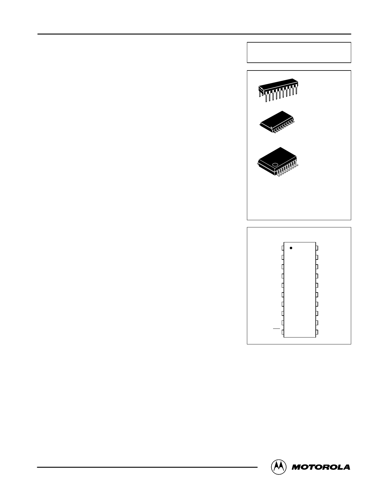
MC14LC5480
20
1
20
1
P SUFFIX
PLASTIC DIP
CASE 738
DW SUFFIX
SOG PACKAGE
CASE 751D
SD SUFFIX
SSOP
20 CASE 940C
1
ORDERING INFORMATION
MC14LC5480P Plastic DIP
MC14LC5480DW SOG Package
MC14LC5480SD SSOP
PIN ASSIGNMENT
RO+
RO–
PI
PO–
PO+
VDD
FSR
DR
BCLKR
PDI
1
2
3
4
5
6
7
8
9
10
20 VAG
19 TI+
18 TI–
17 TG
16 Mu/A
15 VSS
14 FST
13 DT
12 BCLKT
11 MCLK
This document contains information on a new product. Specifications and information herein are subject to change without notice.
REV 0.1
5/96
©MOMoTtoOroRla,OInLc.A1996
MC14LC5480
1
1 page 
version algorithm. All of the analog circuitry involved in the
data conversion (the voltage reference, RDAC, CDAC, and
comparator) are implemented with a differential architecture.
The receive section includes the DAC described above, a
sample and hold amplifier, a 5–pole, 3400 Hz switched ca-
pacitor low–pass filter with sinX/X correction, and a 2–pole
active smoothing filter to reduce the spectral components of
the switched capacitor filter. The output of the smoothing fil-
ter is buffered by an amplifier, which is output at the RO+ and
RO– pins. These outputs are capable of driving a 4 kΩ load
differentially or a 2 kΩ load to the VAG pin. The MC14LC5480
also has a pair of power amplifiers that are connected in a
push–pull configuration. The PI pin is the inverting input to
the PO– power amplifier. The non–inverting input is internally
tied to the VAG pin. This allows this amplifier to be used in an
inverting gain circuit with two external resistors. The PO+
amplifier has a gain of minus one, and is internally con-
nected to the PO– output. This complete power amplifier cir-
cuit is a differential (push–pull) amplifier with adjustable gain
that is capable of driving a 300 Ω load to +12 dBm. The
power amplifier may be powered down independently of the
rest of the chip by connecting the PI pin to VDD.
POWER–DOWN
There are two methods of putting this device into a low
power consumption mode, which makes the device nonfunc-
tional and consumes virtually no power. PDI is the power–
down input pin which, when taken low, powers down the
device. Another way to power the device down is to hold both
the FST and FSR pins low. When the chip is powered down,
the VAG, TG, RO+, RO–, PO+, PO–, and DT outputs are high
impedance. To return the chip to the power–up state, PDI
must be high and the FST frame sync pulse must be present.
The DT output will remain in a high–impedance state for at
least two FST pulses after power–up.
MASTER CLOCK
Since this codec–filter design has a single DAC architec-
ture, the MCLK pin is used as the master clock for all analog
signal processing including analog–to–digital conversion,
digital–to–analog conversion, and for transmit and receive fil-
tering functions of this device. The clock frequency applied to
the MCLK pin may be 256 kHz, 512 kHz, 1.536 MHz,
1.544 MHz, 2.048 MHz, 2.56 MHz, or 4.096 MHz. This de-
vice has a prescaler that automatically determines the proper
divide ratio to use for the MCLK input, which achieves the re-
quired 256 kHz internal sequencing clock. The clocking re-
quirements of the MCLK input are independent of the PCM
data transfer mode (i.e., Long Frame Sync, Short Frame
Sync, IDL mode, or GCI mode).
DIGITAL I/O
The MC14LC5480 is pin selectable for Mu–Law or A–Law.
Table 1 shows the 8–bit data word format for positive and
negative zero and full scale for both companding schemes
(see Tables 3 and 4 at the end of this document for a com-
plete PCM word conversion table). Table 2 shows the series
of eight PCM words for both Mu–Law and A–Law that corre-
spond to a digital milliwatt. The digital mW is the 1 kHz cal-
ibration signal reconstructed by the DAC that defines the
absolute gain or 0 dBm0 Transmission Level Point (TLP) of
the DAC. The 0 dBm0 level for Mu–Law is 3.17 dB below the
maximum level for an unclipped tone signal. The 0 dBm0
level for A–Law is 3.14 dB below the maximum level for an
unclipped tone signal. The timing for the PCM data transfer is
independent of the companding scheme selected. Refer to
Figure 2 for a summary and comparison of the four PCM
data interface modes of this device.
Level
+ Full Scale
+ Zero
– Zero
– Full Scale
Sign Bit
1
1
0
0
Table 1. PCM Codes for Zero and Full Scale
Mu–Law
Chord Bits
Step Bits
Sign Bit
000
0000
1
111
1111
1
111
1111
0
000
0000
0
A–Law
Chord Bits
010
101
101
010
Step Bits
1010
0101
0101
1010
Phase
π/8
3π/8
5π/8
7π/8
9π/8
11π/8
13π/8
15π/8
Sign Bit
0
0
0
0
1
1
1
1
Table 2. PCM Codes for Digital mW
Mu–Law
Chord Bits
Step Bits
Sign Bit
001
1110
0
000
1011
0
000
1011
0
001
1110
0
001
1110
1
000
1011
1
000
1011
1
001
1110
1
A–Law
Chord Bits
011
010
010
011
011
010
010
011
Step Bits
0100
0001
0001
0100
0100
0001
0001
0100
MOTOROLA
MC14LC5480
5
5 Page 
ANALOG ELECTRICAL CHARACTERISTICS (VDD = + 5 V ± 5%, VSS = 0 V, TA = – 40 to + 85°C)
Characteristics
Min Typ
Input Current
TI+, TI–
—
± 0.1
Input Resistance to VAG (VAG – 0.5 V ≤ Vin ≤ VAG + 0.5 V)
Input Capacitance
TI+, TI–
TI+, TI–
10
—
—
—
Input Offset Voltage of TG Op Amp
TI+, TI–
—
—
Input Common Mode Voltage Range
TI+, TI–
1.2
Input Common Mode Rejection Ratio
TI+, TI–
—
60
Gain Bandwidth Product (10 kHz) of TG Op Amp (RL ≥ 10 kΩ)
DC Open Loop Gain of TG Op Amp (RL ≥ 10 kΩ)
Equivalent Input Noise (C–Message) Between TI+ and TI– at TG
— 3000
— 95
— – 30
Output Load Capacitance for TG Op Amp
0—
Output Voltage Range for TG
(RL = 10 kΩ to VAG)
(RL = 2 kΩ to VAG)
Output Current (0.5 V ≤ Vout ≤ VDD – 0.5 V)
Output Load Resistance to VAG
Output Impedance (0 to 3.4 kHz)
TG, RO+, RO–
TG, RO+, and RO–
RO+ or RO–
0.5
1.0
± 1.0
2
—
—
—
—
—
1
Output Load Capacitance
RO+ or RO–
0
—
DC Output Offset Voltage of RO+ or RO– Referenced to VAG
—
VAG Output Voltage Referenced to VSS (No Load)
2.2
VAG Output Current with ± 25 mV Change in Output Voltage
± 2.0
Power Supply Rejection Ratio
(0 to 100 kHz @100 mVrms Applied to VDD,
C–Message Weighting, All Analog Signals
Referenced to VAG Pin)
Transmit
Receive
50
50
Power Drivers PI, PO+, PO–
—
2.4
± 10
80
75
Input Current (VAG – 0.5 V ≤ PI ≤ VAG + 0.5 V)
Input Resistance (VAG – 0.5 V ≤ PI ≤ VAG + 0.5 V)
Input Offset Voltage
PI —
PI 10
PI —
± 0.05
—
—
Output Offset Voltage of PO+ Relative to PO– (Inverted Unity Gain for PO–)
—
—
Output Current (VSS + 0.7 V ≤ PO+ or PO– ≤ VDD – 0.7 V)
PO+ or PO– Output Resistance (Inverted Unity Gain for PO–)
± 10 —
—1
Gain Bandwidth Product (10 kHz, Open Loop for PO–)
— 1000
Load Capacitance (PO+ or PO– to VAG, or PO+ to PO–)
Gain of PO+ Relative to PO– (RL = 300 Ω, + 3 dBm0, 1 kHz)
Total Signal to Distortion at PO+ and PO– with a 300 Ω Differential Load
0
– 0.2
45
—
0
60
Power Supply Rejection Ratio
(0 to 25 kHz @ 100 mVrms Applied to VDD.
PO– Connected to PI. Differential or Measured
Referenced to VAG Pin.)
0 to 4 kHz
4 to 25 kHz
40
—
55
40
NOTE: Bold type indicates a change from the MC145480 to the MC14LC5480.
Max
± 1.0
—
10
±5
VDD – 2.0
—
—
—
—
100
VDD – 0.5
VDD – 1.0
—
—
—
500
± 25
2.6
—
—
—
Unit
µA
MΩ
pF
mV
V
dB
kHz
dB
dBrnC
pF
V
mA
kΩ
Ω
pF
mV
V
mA
dBC
± 1.0
—
± 20
± 50
—
—
—
1000
+ 0.2
—
—
—
µA
MΩ
mV
mV
mA
Ω
kHz
pF
dB
dBC
dB
MOTOROLA
MC14LC5480
11
11 Page | ||
| Páginas | Total 24 Páginas | |
| PDF Descargar | [ Datasheet MC14LC5480.PDF ] | |
Hoja de datos destacado
| Número de pieza | Descripción | Fabricantes |
| MC14LC5480 | 5 V PCM Codec-Filter | Motorola Semiconductors |
| MC14LC5480 | 5 V PCM Codec-Filter | Motorola Semiconductors |
| Número de pieza | Descripción | Fabricantes |
| SLA6805M | High Voltage 3 phase Motor Driver IC. |
Sanken |
| SDC1742 | 12- and 14-Bit Hybrid Synchro / Resolver-to-Digital Converters. |
Analog Devices |
|
DataSheet.es es una pagina web que funciona como un repositorio de manuales o hoja de datos de muchos de los productos más populares, |
| DataSheet.es | 2020 | Privacy Policy | Contacto | Buscar |