|
|
|
PDF ICS9248-126 Data sheet ( Hoja de datos )
| Número de pieza | ICS9248-126 | |
| Descripción | Frequency Generator & Integrated Buffers | |
| Fabricantes | Integrated Circuit Systems | |
| Logotipo | ||
Hay una vista previa y un enlace de descarga de ICS9248-126 (archivo pdf) en la parte inferior de esta página. Total 12 Páginas | ||
|
No Preview Available !
Integrated
Circuit
Systems, Inc.
ICS9248-126
Frequency Generator & Integrated Buffers for Celeron & PII/III™ & K6
Recommended Application:
Motherboard Single chip clock solution for Pentium II/III and
K6 processors, using SIS540/SIS630 style chipset.
Output Features:
• 3- CPUs @ 2.5/3.3V, up to 166MHz.
• 14 - SDRAM @ 3.3V
• 7- PCI @3.3V,
• 1- 48MHz, @3.3V fixed.
• 1- 24/48MHz, @3.3V selectable by I2C
(Default is 24MHz).
• 2- REF @3.3V, 14.318MHz.
Features:
• Up to 166MHz frequency support
• Support FS0-FS3 trapping status bit for I2C read back.
• Support power management: CPU, PCI, SDRAM stop
and Power down Mode form I2C programming.
• Spread spectrum for EMI control (0 to -0.5%, ± 0.25%).
• FS0, FS1, FS3 must have a internal 120K pull-Down
to GND.
• Uses external 14.318MHz crystal
Skew Specifications:
• CPU - CPU: < 175ps
• SDRAM - SDRAM < 500ps
• PCI - PCI: < 500ps
• CPU - SDRAM: < 500ps
• CPU - PCI: 1 - 4ns
Pin Configuration
VDDREF
*1REF0/FS3
GND
X1
X2
VDDPCI
*PCICLK0/FS1
*PCICLK1/FS2
PCICLK2
GND
PCICLK3
PCICLK4
PCICLK5
PCICLK6
VDDSDR
GND
SDRAM0
SDRAM1
VDDSDR
SDRAM2
SDRAM3
GND
SDATA
SCLK
1
2
3
4
5
6
7
8
9
10
11
12
13
14
15
16
17
18
19
20
21
22
23
24
48 REF1
47 VDDLCPU
46 CPUCLK0
45 CPUCLK1
44 GND
43 CPUCLK2
42 VDDSDR
41 SDRAM13
40 SDRAM12
39 GND
38 SDRAM11
37 SDRAM10
36 VDDSDR
35 SDRAM9
34 SDRAM8
33 GNDSDR
32 SDRAM7
31 SDRAM6
30 VDDSDR
29 SDRAM5
28 SDRAM4
27 VDDSDR
26 48MHz/FS0*1
25 24_48MHz/CPU2.5_3.3#*
48-Pin 300mil SSOP
* These inputs have a 120K pull down to GND.
1 These are double strength.
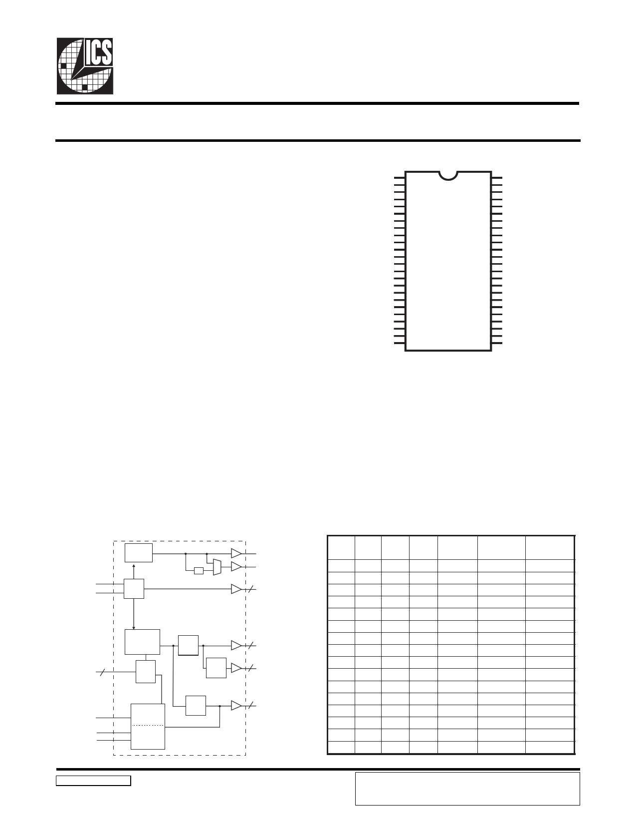
Block Diagram
PLL2
X1 XTAL
X2 OSC
48MHz
/ 2 24_48MHz
2 REF (1:0)
FS(3:0) 4
CPU2.5_3.3#
SDATA
SCLK
PLL1
Spread
Spectrum
LATCH
CPU
CLOCK
DIVDER
SDRAM
CLOCK
DIVDER
Control
Logic
Config.
Reg.
PCI
CLOCK
DIVDER
3 CPUCLK (2:0)
14 SDRAM (13:0)
PCICLK (6:0)
7
Functionality
FS3 FS2
FS1
FS0
CPU
(MHz)
SDRAM
(MHz)
PCICLK
(MHz)
0 0 0 0 66.6
100.0
33.3
0 0 0 1 100.0 100.0
33.3
0 0 1 0 150.0 100.0
37.5
0 0 1 1 133.3 100.0
33.3
0 1 0 0 66.8 133.6
33.4
0 1 0 1 100.0 133.3
33.3
0 1 1 0 100.0 150.0
37.5
0 1 1 1 133.3 133.3
33.3
1 0 0 0 66.8
66.8
33.4
1 0 0 1 97.0
97.0
32.3
1 0 1 0 70.0
105.0
35.0
1 0 1 1 95.0
95.0
31.7
1 1 0 0 95.0
126.7
31.7
1 1 0 1 112.0 112.0
37.3
1 1 1 0 97.0
129.3
32.2
1 1 1 1 96.2
96.2
32.1
9248-126 Rev C 9/6/00
Third party brands and names are the property of their respective owners.
ICS reserves the right to make changes in the device data identified in
this publication without further notice. ICS advises its customers to
obtain the latest version of all device data to verify that any
information being relied upon by the customer is current and accurate.
1 page 
ICS9248-126
Byte 1: CPU, Active/Inactive Register
(1= enable, 0 = disable)
BIT
Bit 7
Bit 6
Bit 5
Bit 4
Bit 3
Bit 2
Bit 1
Bit 0
PIN#
-
-
-
-
43
45
46
-
PWD
DESCRIPTION
SEL24_48#
1 (48MHz when set to 0)
(24MHz when set to 1)
1 Reserved
1 Reserved
1 Reserved
1 CPUCLK2 (Act/Inact)
1 CPUCLK1 (Act/Inact)
1 CPUCLK0 (Act/Inact)
1 Reserved
Byte 2: PCI, Active/Inactive Register
(1= enable, 0 = disable)
BIT
Bit 7
Bit 6
Bit 5
Bit 4
Bit 3
Bit 2
Bit 1
Bit 0
PIN#
-
14
13
12
11
9
8
7
PWD
DESCRIPTION
1 (CPU2.5_3.3#)
1 PCICLK6 (Act/Inact)
1 PCICLK5 (Act/Inact)
1 PCICLK4 (Act/Inact)
1 PCICLK3 (Act/Inact)
1 PCICLK2 (Act/Inact)
1 PCICLK1 (Act/Inact)
1 PCICLK0 (Act/Inact)
Byte 3: SDRAM, Active/Inactive Register
(1= enable, 0 = disable)
BIT
Bit 7
Bit 6
Bit 5
Bit 4
Bit 3
Bit 2
Bit 1
Bit 0
PIN#
32
31
29
28
21
20
18
17
PWD
DESCRIPTION
1 SDRAM 7 (Act/Inact)
1 SDRAM 6 (Act/Inact)
1 SDRAM 5 (Act/Inact)
1 SDRAM 4 (Act/Inact)
1 SDRAM 3 (Act/Inact)
1 SDRAM 2 (Act/Inact)
1 SDRAM 1 (Act/Inact)
1 SDRAM 0 (Act/Inact)
Byte 4: Reserved , Active/Inactive Register
(1= enable, 0 = disable)
BIT
Bit 7
Bit 6
Bit 5
Bit 4
Bit 3
Bit 2
Bit 1
Bit 0
PIN#
25
26
41
40
38
37
35
34
PWD
DESCRIPTION
1 24_48MHz
1 48MHz
1 SDRAM13
1 SDRAM12
1 SDRAM11
1 SDRAM10
1 SDRAM9
1 SDRAM8
Byte 5: Peripheral , Active/Inactive Register
(1= enable, 0 = disable)
BIT
Bit 7
Bit 6
Bit 5
Bit 4
Bit 3
Bit 2
Bit 1
Bit 0
PIN#
-
-
-
-
-
-
48
2
PWD
DESCRIPTION
1 Reserved
1 Reserved
1 FS3#
1 FS2#
1 FS1#
1 FS0#
1 REF1 (Act/Inact)
1 REF0 (Act/Inact)
Notes:
1. Inactive means outputs are held LOW and are disabled
from switching.
2. Latched Frequency Selects (FS#) will be inferted logic
load of the input frequency select pin conditions.
Byte 6: Peripheral , Active/Inactive Register
(1= enable, 0 = disable)
BIT PIN# PWD
DESCRIPTION
Bit7 -
0 Reserved (Note)
Bit6 -
0 Reserved (Note)
Bit5 -
0 Reserved (Note)
Bit4 -
0 Reserved (Note)
Bit3 -
0 Reserved (Note)
Bit2 -
1 Reserved (Note)
Bit1 -
1 Reserved (Note)
Bit0 -
0 Reserved (Note)
Note: Dont write into this register, writing into this
register can cause malfunction
Third party brands and names are the property of their respective owners.
5
5 Page 
ICS9248-126
General Layout Precautions:
1) Use a ground plane on the top routing
layer of the PCB in all areas not used
by traces.
2) Make all power traces and ground
traces as wide as the via pad for lower
inductance.
VDD
Notes:
1 All clock outputs should have
provisions for a 15pf capacitor
between the clock output and series
terminating resistor. Not shown in all
places to improve readability of
diagram.
2 Optional crystal load capacitors are
recommended. They should be
included in the layout but not
inserted unless needed.
Component Values:
C1 : Crystal load values determined by user
C2 : 22µF/20V/D case/Tantalum
AVX TAJD226M020R
C3 : 15pF capacitor
FB = Fair-Rite products 2512066017X1
All unmarked capacitors are 0.01µF ceramic
Ferrite
Bead
C1
C1
2
3.3V Power Route
C2
22µF/20V
Tantalum
1
2
3
4
5
6
7
8
9
10
11
12
13
14
15
16
17
18
19
20
21
22
23
24
C2
22µF/20V
Tantalum
Ferrite
Bead
VDD
48
47
46
45
C3
44
43
42
41
40
39
38
37
36
35
34
33
32
31
30
29
28
27
26
25
2.5V Power Route
C3
1
Clock Load
Ground
3.3V Power Route
Connections to VDD:
= Routed Power
= Ground Connection Key (component side copper)
= Ground Plane Connection
= Power Route Connection
= Solder Pads
= Clock Load
Third party brands and names are the property of their respective owners.
11
11 Page | ||
| Páginas | Total 12 Páginas | |
| PDF Descargar | [ Datasheet ICS9248-126.PDF ] | |
Hoja de datos destacado
| Número de pieza | Descripción | Fabricantes |
| ICS9248-126 | Frequency Generator & Integrated Buffers | Integrated Circuit Systems |
| ICS9248-127 | Frequency Generator & Integrated Buffers | Integrated Circuit Systems |
| ICS9248-128 | Frequency Generator & Integrated Buffers | Integrated Circuit Systems |
| Número de pieza | Descripción | Fabricantes |
| SLA6805M | High Voltage 3 phase Motor Driver IC. |
Sanken |
| SDC1742 | 12- and 14-Bit Hybrid Synchro / Resolver-to-Digital Converters. |
Analog Devices |
|
DataSheet.es es una pagina web que funciona como un repositorio de manuales o hoja de datos de muchos de los productos más populares, |
| DataSheet.es | 2020 | Privacy Policy | Contacto | Buscar |