|
|
|
PDF MTB36N06E Data sheet ( Hoja de datos )
| Número de pieza | MTB36N06E | |
| Descripción | TMOS POWER FET 36 AMPERES 60 VOLTS | |
| Fabricantes | Motorola Semiconductors | |
| Logotipo | ||
Hay una vista previa y un enlace de descarga de MTB36N06E (archivo pdf) en la parte inferior de esta página. Total 10 Páginas | ||
|
No Preview Available !
MOTOROLA
SEMICONDUCTOR TECHNICAL DATA
Order this document
by MTB36N06E/D
™Designer's Data Sheet
TMOS E-FET.™
High Energy Power FET
D2PAK for Surface Mount
N–Channel Enhancement–Mode Silicon Gate
The D2PAK package has the capability of housing a larger die
than any existing surface mount package which allows it to be used
in applications that require the use of surface mount components
with higher power and lower RDS(on) capabilities. This advanced
TMOS E–FET is designed to withstand high energy in the
avalanche and commutation modes. The new energy efficient
design also offers a drain–to–source diode with a fast recovery
time. Designed for low voltage, high speed switching applications in
power supplies, converters and PWM motor controls, these
devices are particularly well suited for bridge circuits where diode
speed and commutating safe operating areas are critical and offer
additional safety margin against unexpected voltage transients.
D
• Avalanche Energy Specified
• Source–to–Drain Diode Recovery Time Comparable to a
G
Discrete Fast Recovery Diode
• Diode is Characterized for Use in Bridge Circuits
• IDSS and VDS(on) Specified at Elevated Temperature
• Short Heatsink Tab Manufactured — Not Sheared
• Specially Designed Leadframe for Maximum Power Dissipation
• Available in 24 mm 13–inch/800 Unit Tape & Reel, Add T4 Suffix to Part Number
®
S
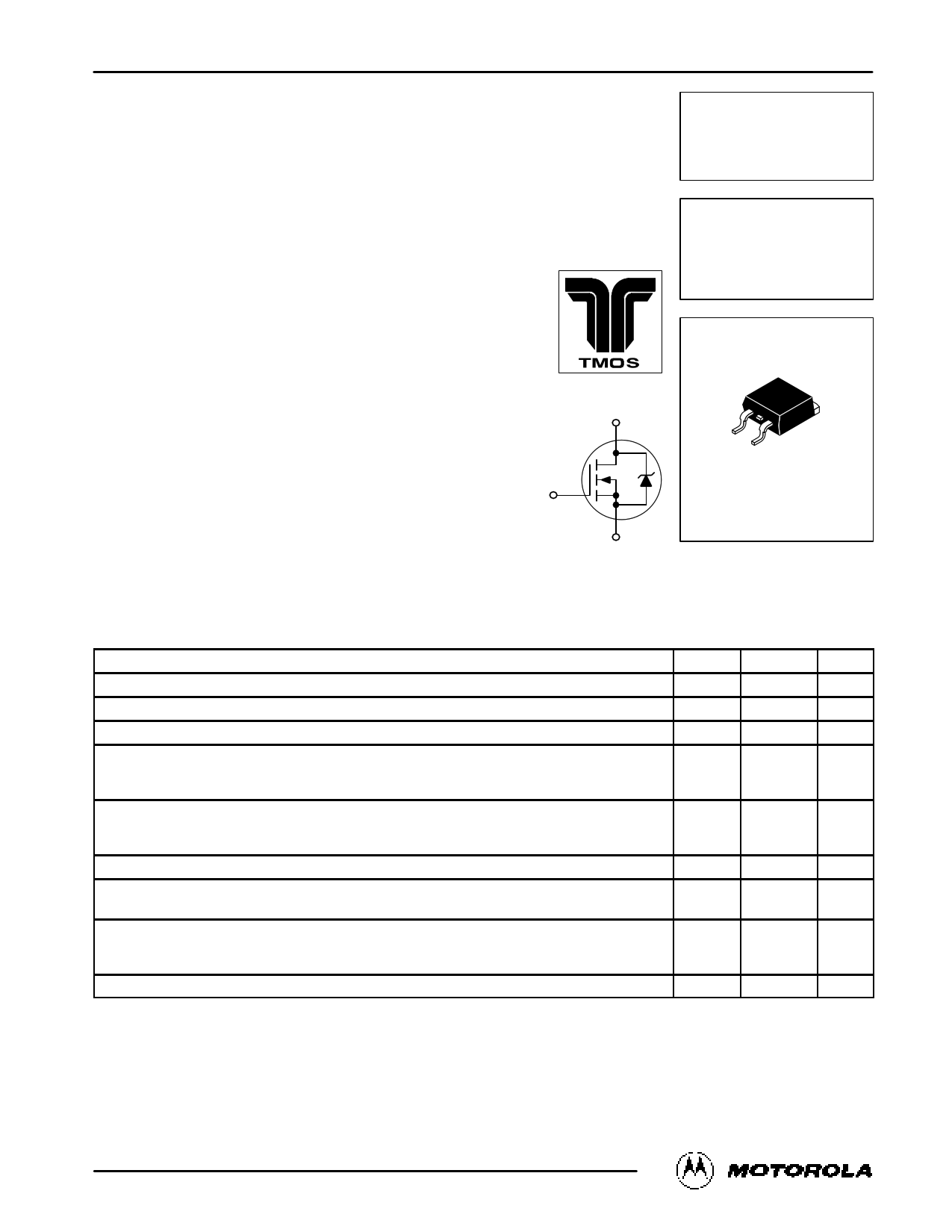
MTB36N06E
Motorola Preferred Device
TMOS POWER FET
36 AMPERES
60 VOLTS
RDS(on) = 0.04 OHM
CASE 418B–02, Style 2
D2PAK
MAXIMUM RATINGS (TC = 25°C unless otherwise noted)
Rating
Symbol
Value
Unit
Drain–to–Source Voltage
VDSS 60 Vdc
Drain–to–Gate Voltage (RGS = 1.0 MΩ)
VDGR 60 Vdc
Gate–to–Source Voltage — Continuous
VGS
± 20 Vdc
Drain Current — Continuous
Drain Current — Continuous @ 100°C
Drain Current — Single Pulse (tp ≤ 10 µs)
ID 36 Amps
ID 22
IDM 144 Apk
Total Power Dissipation
Derate above 25°C
Total Power Dissipation @ TA = 25°C, when mounted with the minimum recommended pad size
PD 100 Watts
0.80 W/°C
2.5 Watts
Operating and Storage Temperature Range
TJ, Tstg – 55 to 150 °C
Single Pulse Drain–to–Source Avalanche Energy — Starting TJ = 25°C
(VDD = 25 Vdc, VGS = 10 Vpk, IL = 36 Apk, L = 0.34 mH, RG = 25 Ω)
EAS 220 mJ
Thermal Resistance — Junction to Case
Thermal Resistance — Junction to Ambient
Thermal Resistance — Junction to Ambient, when mounted with the minimum recommended pad size
RθJC
RθJA
RθJA
1.25 °C/W
62.5
50
Maximum Lead Temperature for Soldering Purposes, 1/8″ from case for 10 seconds
TL 260 °C
Designer’s Data for “Worst Case” Conditions — The Designer’s Data Sheet permits the design of most circuits entirely from the information presented. SOA Limit
curves — representing boundaries on device characteristics — are given to facilitate “worst case” design.
E–FET and Designer’s are trademarks of Motorola, Inc. TMOS is a registered trademark of Motorola, Inc.
Thermal Clad is a trademark of the Bergquist Company
Preferred devices are Motorola recommended choices for future use and best overall value.
©MMoottoororolal,aInTc.M19O9S4 Power MOSFET Transistor Device Data
1
1 page 
20
VDS
16
50
40
12
8
Q1
4
Q3
QT
Q2
ID = 36 A
VDS = 48 V
TJ = 25°C
30
20
10
00
0 10 20 30 40 50 60
QT, TOTAL CHARGE (nC)
Figure 8. Gate–To–Source and Drain–To–Source
Voltage versus Total Charge
MTB36N06E
10000
4000
2000
1000
VDD = 30 V
ID = 36 A
VGS = 10 V
TJ = 25°C
400
200
100
tf
tr
td(off)
td(on)
40
20
10
10 20
40 100 200 400
RG, GATE RESISTANCE (OHMS)
1000
Figure 9. Resistive Switching Time
Variation versus Gate Resistance
DRAIN–TO–SOURCE DIODE CHARACTERISTICS
50
45 VGS = 0 V
40 TJ = 25°C
35
30
25
20
15
10
5
0 0.2 0.4 0.6 0.8 1 1.2 1.4 1.6 1.8 2
VSD, SOURCE–TO–DRAIN VOLTAGE (VOLTS)
Figure 10. Diode Forward Voltage versus Current
SAFE OPERATING AREA
The Forward Biased Safe Operating Area curves define
the maximum simultaneous drain–to–source voltage and
drain current that a transistor can handle safely when it is for-
ward biased. Curves are based upon maximum peak junc-
tion temperature and a case temperature (TC) of 25°C. Peak
repetitive pulsed power limits are determined by using the
thermal response data in conjunction with the procedures
discussed in AN569, “Transient Thermal Resistance–Gener-
al Data and Its Use.”
Switching between the off–state and the on–state may tra-
verse any load line provided neither rated peak current (IDM)
nor rated voltage (VDSS) is exceeded and the transition time
(tr,tf) do not exceed 10 µs. In addition the total power aver-
aged over a complete switching cycle must not exceed
(TJ(MAX) – TC)/(RθJC).
A Power MOSFET designated E–FET can be safely used
in switching circuits with unclamped inductive loads. For reli-
able operation, the stored energy from circuit inductance dis-
sipated in the transistor while in avalanche must be less than
the rated limit and adjusted for operating conditions differing
from those specified. Although industry practice is to rate in
terms of energy, avalanche energy capability is not a con-
stant. The energy rating decreases non–linearly with an in-
crease of peak current in avalanche and peak junction
temperature.
Although many E–FETs can withstand the stress of drain–
to–source avalanche at currents up to rated pulsed current
(IDM), the energy rating is specified at rated continuous cur-
rent (ID), in accordance with industry custom. The energy rat-
ing must be derated for temperature as shown in the
accompanying graph (Figure 12). Maximum energy at cur-
rents below rated continuous ID can safely be assumed to
equal the values indicated.
Motorola TMOS Power MOSFET Transistor Device Data
5
5 Page | ||
| Páginas | Total 10 Páginas | |
| PDF Descargar | [ Datasheet MTB36N06E.PDF ] | |
Hoja de datos destacado
| Número de pieza | Descripción | Fabricantes |
| MTB36N06E | TMOS POWER FET 36 AMPERES 60 VOLTS | Motorola Semiconductors |
| MTB36N06V | TMOS POWER FET 32 AMPERES 60 VOLTS | Motorola Semiconductors |
| MTB36N06V | Power MOSFET ( Transistor ) | ON Semiconductor |
| Número de pieza | Descripción | Fabricantes |
| SLA6805M | High Voltage 3 phase Motor Driver IC. |
Sanken |
| SDC1742 | 12- and 14-Bit Hybrid Synchro / Resolver-to-Digital Converters. |
Analog Devices |
|
DataSheet.es es una pagina web que funciona como un repositorio de manuales o hoja de datos de muchos de los productos más populares, |
| DataSheet.es | 2020 | Privacy Policy | Contacto | Buscar |