|
|
|
PDF MAX3890 Data sheet ( Hoja de datos )
| Número de pieza | MAX3890 | |
| Descripción | +3.3V / 2.5Gbps / SDH/SONET 16:1 Serializer with Clock Synthesis and LVDS Inputs | |
| Fabricantes | Maxim Integrated | |
| Logotipo | ||
Hay una vista previa y un enlace de descarga de MAX3890 (archivo pdf) en la parte inferior de esta página. Total 12 Páginas | ||
|
No Preview Available !
19-1498; Rev 0; 6/99
EVAALVUAAILTAIOBNLEKIT
+3.3V, 2.5Gbps, SDH/SONET 16:1 Serializer
with Clock Synthesis and LVDS Inputs
General Description
The MAX3890 serializer is ideal for converting 16-bit-
wide, 155Mbps parallel data to 2.5Gbps serial data in
ATM and SDH/SONET applications. Operating from a
single +3.3V supply, this device accepts low-voltage
differential-signal (LVDS) clock and data inputs for
interfacing with high-speed digital circuitry, and deliv-
ers PECL serial data and clock outputs. A fully integrat-
ed PLL synthesizes an internal 2.5GHz serial clock from
a 155.52MHz, 77.76MHz, 51.84MHz, or 38.88MHz ref-
erence clock. A loopback data output is provided to
facilitate system diagnostic testing.
The MAX3890 is available in the extended temperature
range (-40°C to +85°C) in a 64-pin TQFP exposed-
paddle (EP) package.
Features
o Single +3.3V Supply
o 495mW Power Consumption
o Exceeds ANSI, ITU, and Bellcore Specifications
o 155Mbps (16-bit wide) Parallel to 2.5Gbps Serial
Conversion
o Clock Synthesis for 2.5Gbps
o Multiple Clock Reference Frequencies
(155.52MHz, 77.76MHz, 51.84MHz, 38.88MHz)
o LVDS Parallel Clock and Data Inputs
o Additional High-Speed Output for System
Loopback Testing
Applications
2.5Gbps SDH/SONET Transmission Systems
2.5Gbps ATM/SONET Access Nodes
Add/Drop Multiplexers
Digital Cross-Connects
ATM Backplanes
Ordering Information
PART
TEMP. RANGE
MAX3890ECB
-40°C to +85°C
*EP = Exposed Paddle
PIN-PACKAGE
64 TQFP-EP*
Pin Configuration appears at end of data sheet.
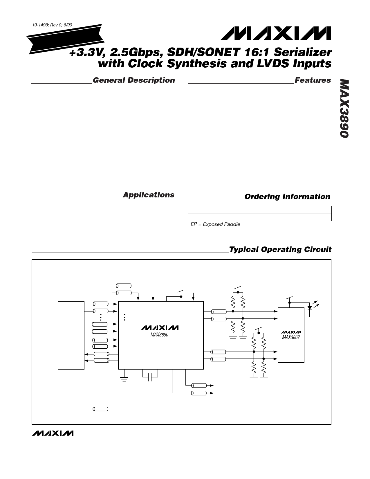
Typical Operating Circuit
155MHz REF. CLOCK INPUT
+3.3V TTL
OVERHEAD
GENERATION
PDI0+ RCLK+ RCLK- CLKSET VCC SOS
PDI0-
SDO+
SDO-
PDI15+
PDI15-
PCLKI+
MAX3890
PCLKI-
PCLKO+
PCLKO-
GND
FIL+
SCLKO+
SCLKO-
FIL- SLBO+ SLBO-
+3.3V
130Ω
130Ω
+3.3V
VCC
82Ω 82Ω +3.3V
MAX3867
130Ω
130Ω
82Ω 82Ω
330nF
THIS SYMBOL REPRESENTS A TRANSMISSION LINE
OF CHARACTERISTIC IMPEDANCE (Z0 = 50Ω).
OPTIONAL CONNECTION TO MAX3880
FOR SYSTEM LOOPBACK TESTING.
________________________________________________________________ Maxim Integrated Products 1
For free samples & the latest literature: http://www.maxim-ic.com, or phone 1-800-998-8800.
For small orders, phone 1-800-835-8769.
1 page 
+3.3V, 2.5Gbps, SDH/SONET 16:1 Serializer
with Clock Synthesis and LVDS Inputs
PIN
1, 17, 33, 48, 49, 63
2, 5, 7, 10, 13,
14, 32, 56, 60, 64
3
4
6
8
9
11
12
15
NAME
GND
VCC
SLBO-
SLBO+
SOS
SCLKO-
SCLKO+
SDO-
SDO+
PCLKI+
16
18, 20, 22, 24, 26,
28, 30, 34, 36, 38,
40, 42, 44, 46, 50, 52
19, 21, 23, 25, 27,
29, 31, 35, 37, 39,
41, 43, 45, 47, 51, 53
54
PCLKI-
PDI15+ to
PDI0+
PDI15- to
PDI0-
PCLKO+
55 PCLKO-
57 RCLK+
58 RCLK-
59 CLKSET
61 FIL-
62 FIL+
Pin Description
Ground
FUNCTION
+3.3V Supply Voltage
System Loopback Inverting Output. Enabled when SOS is high.
System Loopback Noninverting Output. Enabled when SOS is high.
System Loopback Output Select. System loopback disabled when low.
Inverting PECL Serial Clock Output
Noninverting PECL Serial Clock Output
Inverting PECL Serial-Data Output
Noninverting PECL Serial-Data Output
Noninverting LVDS Parallel Clock Input. Connect the incoming parallel-clock signal to the
PCLKI inputs. Note that data is updated on the positive transition of the PCLKI signal.
Inverting LVDS Parallel Clock Input. Connect the incoming parallel-clock signal to the PCLKI
inputs. Note that data is updated on the positive transition of the PCLKI signal.
Noninverting LVDS Parallel Data Inputs. Data is clocked on the PCLKI positive transition.
Inverting LVDS Parallel Data Inputs. Data is clocked on the PCLKI positive transition.
Noninverting LVDS Parallel Clock Output. Use positive transition of PCLKO to clock the
overhead management circuit.
Inverting LVDS Parallel Clock Output. Use positive transition of PCLKO to clock the over-
head management circuit.
Noninverting LVDS Reference Clock Input. Connect an LVDS-compatible crystal refer-
ence clock to the RCLK inputs.
Inverting LVDS Reference Clock Input. Connect an LVDS-compatible crystal reference
clock to the RCLK inputs.
Reference Clock Rate Programming Pin:
CLKSET = VCC: Reference Clock Rate = 155.52MHz
CLKSET = Open: Reference Clock Rate = 77.76MHz
CLKSET = 20kΩ to GND: Reference Clock Rate = 51.84MHz
CLKSET = GND: Reference Clock Rate = 38.88MHz
Filter Capacitor Input. Connect a 330nF capacitor between FIL+ and FIL-.
Filter Capacitor Input. Connect a 330nF capacitor between FIL+ and FIL-.
_______________________________________________________________________________________ 5
5 Page 
+3.3V, 2.5Gbps, SDH/SONET 16:1 Serializer
with Clock Synthesis and LVDS Inputs
Package Information
______________________________________________________________________________________ 11
11 Page | ||
| Páginas | Total 12 Páginas | |
| PDF Descargar | [ Datasheet MAX3890.PDF ] | |
Hoja de datos destacado
| Número de pieza | Descripción | Fabricantes |
| MAX389 | High-Voltage / Fault-Protected Analog Multiplexers | Maxim Integrated |
| MAX3890 | +3.3V / 2.5Gbps / SDH/SONET 16:1 Serializer with Clock Synthesis and LVDS Inputs | Maxim Integrated |
| MAX3890ECB | +3.3V / 2.5Gbps / SDH/SONET 16:1 Serializer with Clock Synthesis and LVDS Inputs | Maxim Integrated |
| Número de pieza | Descripción | Fabricantes |
| SLA6805M | High Voltage 3 phase Motor Driver IC. |
Sanken |
| SDC1742 | 12- and 14-Bit Hybrid Synchro / Resolver-to-Digital Converters. |
Analog Devices |
|
DataSheet.es es una pagina web que funciona como un repositorio de manuales o hoja de datos de muchos de los productos más populares, |
| DataSheet.es | 2020 | Privacy Policy | Contacto | Buscar |