|
|
PDF SP3232B Data sheet ( Hoja de datos )
| Número de pieza | SP3232B | |
| Descripción | True +3.0V to +5.5V RS-232 Transceivers | |
| Fabricantes | Sipex | |
| Logotipo |  |
|
Hay una vista previa y un enlace de descarga de SP3232B (archivo pdf) en la parte inferior de esta página. Total 18 Páginas | ||
|
No Preview Available !
® SP3222B/3232B
True +3.0V to +5.5V RS-232 Transceivers
■ Meets true EIA/TIA-232-F Standards
from a +3.0V to +5.5V power supply
■ 250kbps Transmission Rate Under Load
■ 1µA Low-Power Shutdown with Receivers
Active (SP3222B)
■ Interoperable with RS-232 down to +2.7V
power source
■ ESD Specifications:
±2kV Human Body Model
DESCRIPTION
The SP3222B/3232B series is an RS-232 transceiver solution intended for portable or hand-
held applications such as notebook or palmtop computers. The SP3222B/3232B series has
a high-efficiency, charge-pump power supply that requires only 0.1µF capacitors in 3.3V
operation. This charge pump allows the SP3222B/3232B series to deliver true RS-232
performance from a single power supply ranging from +3.0V to +5.5V. The ESD tolerance
of the SP3222B/3232B devices are over ±15kV for both Human Body Model and IEC1000-
4-2 Air discharge test methods. The SP3222B device has a low-power shutdown mode where
the devices' driver outputs and charge pumps are disabled. During shutdown, the supply
current falls to less than 1µA.
SELECTION TABLE
MODEL
SP3222B
SP3232B
Power Supplies
+3.0V to +5.5V
+3.0V to +5.5V
RS-232
Drivers
2
2
RS-232
External
Receivers Components
24
24
Shutdown
Yes
No
TTL No. of
3-State Pins
Yes 18, 20
No 16
Rev. 6/30/03
SP3222B/3232B True +3.0 to +5.5V RS-232 Transceivers
1
© Copyright 2003 Sipex Corporation
1 page 
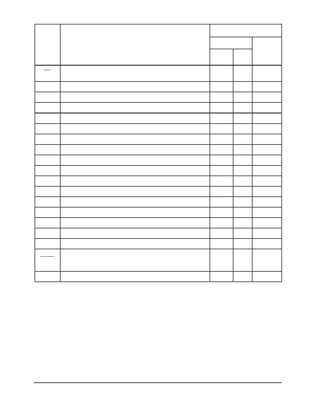
NAME
FUNCTION
EN
Receiver Enable. Apply logic LOW for normal operation.
Apply logic HIGH to disable the receiver outputs (high-Z state).
C1+ Positive terminal of the voltage doubler charge-pump capacitor.
V+ +5.5V generated by the charge pump.
C1- Negative terminal of the voltage doubler charge-pump capacitor.
C2+ Positive terminal of the inverting charge-pump capacitor.
C2- Negative terminal of the inverting charge-pump capacitor.
V- -5.5V generated by the charge pump.
T1OUT RS-232 driver output.
T2OUT RS-232 driver output.
R1IN RS-232 receiver input.
R2IN RS-232 receiver input.
R1OUT TTL/CMOS reciever output.
R2OUT TTL/CMOS reciever output.
T1IN TTL/CMOS driver input.
T2IN TTL/CMOS driver input.
GND Ground.
VCC
SHDN
+3.0V to +5.5V supply voltage
Shutdown Control Input. Drive HIGH for normal device operation.
Drive LOW to shutdown the drivers (high-Z output) and the on-
board power supply.
N.C. No Connect.
Table 1. Device Pin Description
PIN NUMBER
SP3222B
DIP/SO
SSOP
TSSOP
SP3232B
11
-
22
33
44
55
66
77
15 17
88
14 16
99
13 15
10 10
12 13
11 12
16 18
17 19
1
2
3
4
5
6
14
7
13
8
12
9
11
10
15
16
18 20
-
- 11, 14
-
Rev. 6/30/03
SP3222B/3232B True +3.0 to +5.5V RS-232 Transceivers
5
© Copyright 2003 Sipex Corporation
5 Page 
This voltage is regulated to +5.5V. At this
voltage, the internal oscillator is disabled. Si-
multaneous with the transfer of the voltage to
C , the positive side of capacitor C is switched
41
to VCC and the negative side is connected to
GND, allowing the charge pump cycle to begin
again. The charge pump cycle will continue as
long as the operational conditions for the inter-
nal oscillator are present.
Since both V+ and V– are separately generated
from V ; in a no–load condition V+ and V– will
CC
be symmetrical. Older charge pump approaches
that generate V– from V+ will show a decrease in
the magnitude of V– compared to V+ due to the
inherent inefficiencies in the design.
The clock rate for the charge pump typically
operates at 250kHz. The external capacitors can
be as low as 0.1µF with a 16V breakdown
voltage rating.
The Human Body Model has been the generally
accepted ESD testing method for semiconduc-
tors. This method is also specified in MIL-STD-
883, Method 3015.7 for ESD testing. The premise
of this ESD test is to simulate the human body’s
potential to store electrostatic energy and
discharge it to an integrated circuit.
The simulation is performed by using a test
model as shown in Figure 18. This method
will test the IC’s capability to withstand an
ESD transient during normal handling such as
in manufacturing areas where the ICs tend to
be handled frequently.
For the Human Body Model, the current
limiting resistor (RS) and the source capacitor
(CS) are 1.5kΩ and 100pF, respectively.
ESD Tolerance
The SP3222B/3232B series incorporates
ruggedized ESD cells on all driver output and
receiver input pins. The ESD structure is
improved over our previous family for more
rugged applications and environments sensitive
to electrostatic discharges and associated
transients.
VCC = +5V
+
C1 –
–5V
+5V
+
C2 –
–5V
C4
+ – VDD Storage Capacitor
– + VSS Storage Capacitor
C3
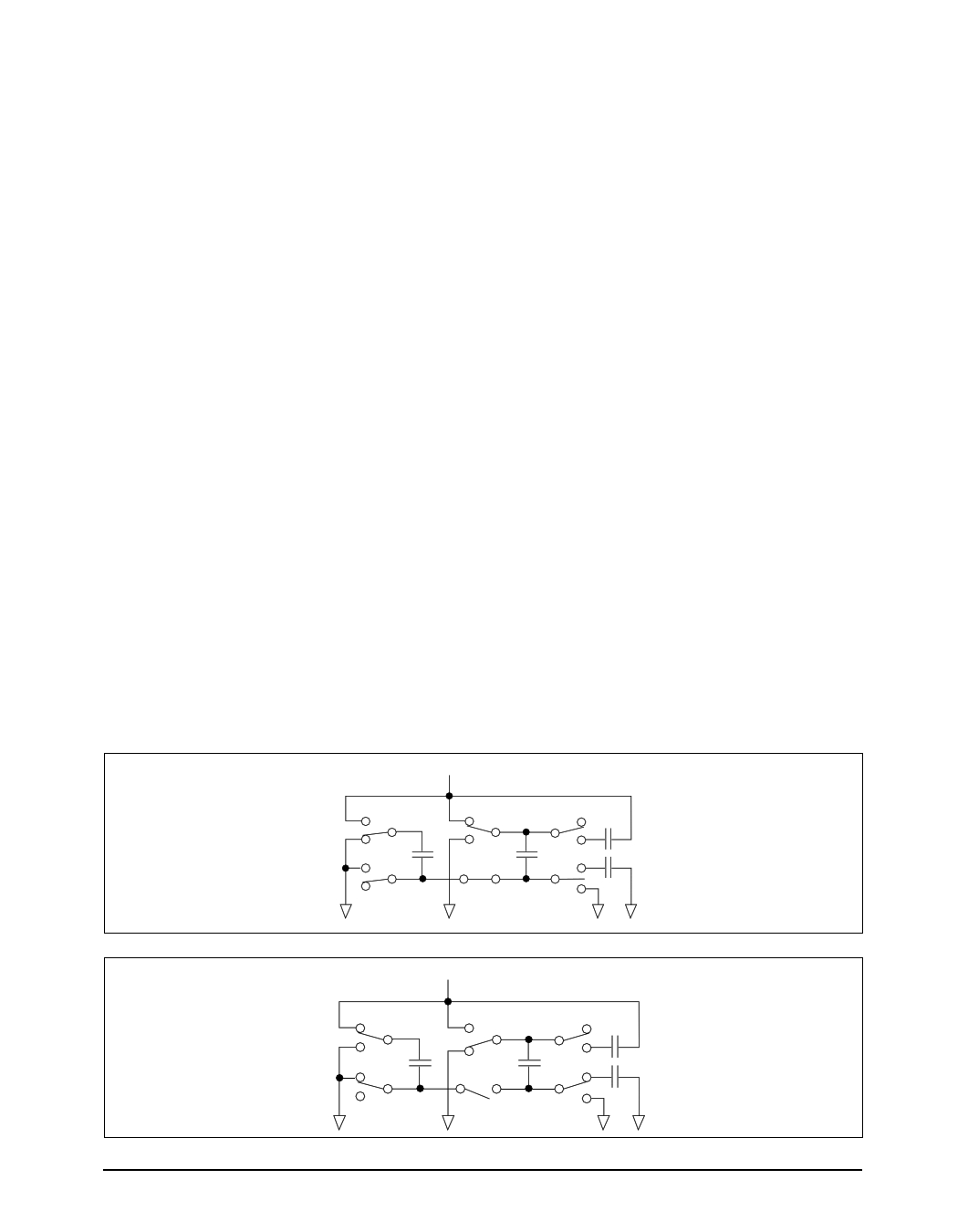
Figure 13. Charge Pump — Phase 1
VCC = +5V
+
C1 –
+
C2 –
–10V
Figure 14. Charge Pump — Phase 2
Rev. 6/30/03
SP3222B/3232B True +3.0 to +5.5V RS-232 Transceivers
11
C4
+ – VDD Storage Capacitor
– + VSS Storage Capacitor
C3
© Copyright 2003 Sipex Corporation
11 Page | ||
| Páginas | Total 18 Páginas | |
| PDF Descargar | [ Datasheet SP3232B.PDF ] | |
Hoja de datos destacado
| Número de pieza | Descripción | Fabricantes |
| SP3232 | 3.3V / 1000 Kbps RS-232 Transceivers | Sipex |
| SP3232B | True +3.0V to +5.5V RS-232 Transceivers | Sipex |
| SP3232E | True +3.0V to +5.5V RS-232 Transceivers | Sipex |
| SP3232E | True +3.0V to +5.5V RS-232 Transceivers | Exar |
| Número de pieza | Descripción | Fabricantes |
| SLA6805M | High Voltage 3 phase Motor Driver IC. |
Sanken |
| SDC1742 | 12- and 14-Bit Hybrid Synchro / Resolver-to-Digital Converters. |
Analog Devices |
|
DataSheet.es es una pagina web que funciona como un repositorio de manuales o hoja de datos de muchos de los productos más populares, |
| DataSheet.es | 2020 | Privacy Policy | Contacto | Buscar |
