|
|
|
PDF PI6C2502AW Data sheet ( Hoja de datos )
| Número de pieza | PI6C2502AW | |
| Descripción | Phase-Locked Loop Clock Driver | |
| Fabricantes | Pericom Semiconductor Corporation | |
| Logotipo | ||
Hay una vista previa y un enlace de descarga de PI6C2502AW (archivo pdf) en la parte inferior de esta página. Total 4 Páginas | ||
|
No Preview Available !
PI6C2502A
111222333444555666777888999000111222333444555666777888999000111222333444555666777888999000111222111222333444555666777888999000111222333444555666777888999000111222333444555666777888999000111222111222333444555666777888999000111222333444555666777888999000111222333444555666777888999000111222111222333444555666777888999000111222333444555666777888999000111222333444555666777888999000111222111222333444555666777888999000111222
Phase-Locked Loop Clock Driver
Product Features
• High-Performance Phase-Locked-Loop Clock Distribution
for Networking,
• Synchronous DRAM modules for server/workstation/
PC applications
• Allows Clock Input to have Spread Spectrum
modulation for EMI reduction
• Zero Input-to-Output delay
• Low jitter: Cycle-to-Cycle jitter ±75ps max.
• On-chip series damping resistor at clock output drivers
for low noise and EMI reduction
• Operates at 3.3V VCC
• Wide range of Clock Frequencies 80 to 134 MHz
• Package: Plastic 8-pin SOIC Package (W)
Product Description
The PI6C2502A features a low-skew, low-jitter, phase-locked loop
(PLL) clock driver. By connecting the feedback FB_OUT output
to the feedback FB_IN input, the propagation delay from the
CLK_IN input to any clock output will be nearly zero.
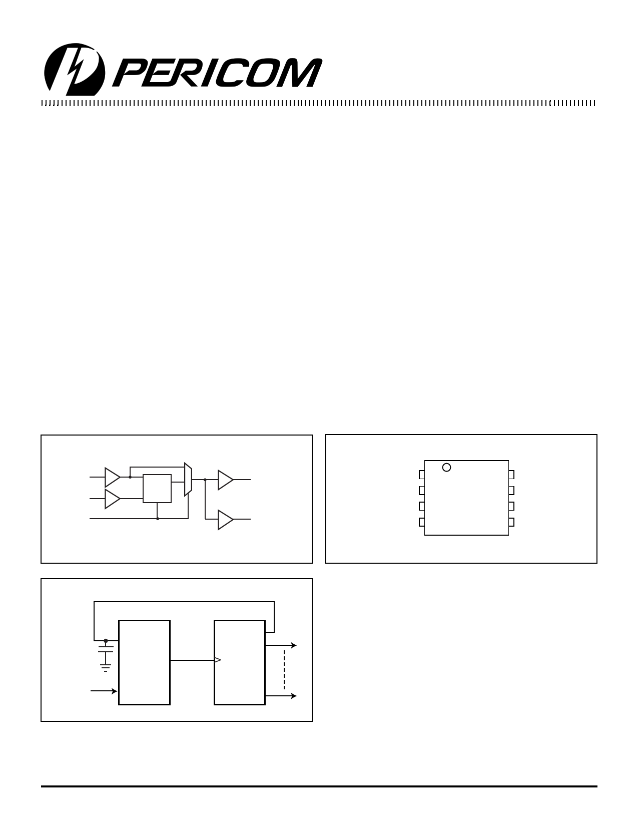
Application
If a system designer needs more than 16 outputs with the features
just described, using two or more zero-delay buffers such as
PI6C2509Q, and PI6C2510Q, is likely to be impractical. The
device-to-device skew introduced can significantly reduce the
performance. Pericom recommends the use of a zero-delay buffer
and an eighteen output non-zero-delay buffer. As shown in Figure
1, this combination produces a zero-delay buffer with all the signal
characteristics of the original zero-delay buffer, but with as many
outputs as the non-zero-delay buffer part. For example, when
combined with an eighteen output non-zero delay buffer, a system
designer can create a seventeen-output zero-delay buffer.
Logic Block Diagram
Product Pin Configuration
CLK_IN
FB_IN
AVCC
PLL
CLK_OUT
FB_OUT
AGND
FB_OUT
CLK_OUT
VCC
1
2
3
4
8-Pin
W
8 CLK_IN
7 AVCC
6 GND
5 FB_IN
Feedback
Reference
Clock
Signal
Zero Delay
Buffer
PI6C2502
CLK_OUT
18 Output
Non-Zero
Delay
Buffer
17
Figure 1. This Combination Provides Zero-Delay Between the
Reference Clocks Signal and 17 Outputs.
1
PS8500
10/02/00
1 page | ||
| Páginas | Total 4 Páginas | |
| PDF Descargar | [ Datasheet PI6C2502AW.PDF ] | |
Hoja de datos destacado
| Número de pieza | Descripción | Fabricantes |
| PI6C2502A | Phase-Locked Loop Clock Driver | Pericom Semiconductor Corporation |
| PI6C2502AW | Phase-Locked Loop Clock Driver | Pericom Semiconductor Corporation |
| Número de pieza | Descripción | Fabricantes |
| SLA6805M | High Voltage 3 phase Motor Driver IC. |
Sanken |
| SDC1742 | 12- and 14-Bit Hybrid Synchro / Resolver-to-Digital Converters. |
Analog Devices |
|
DataSheet.es es una pagina web que funciona como un repositorio de manuales o hoja de datos de muchos de los productos más populares, |
| DataSheet.es | 2020 | Privacy Policy | Contacto | Buscar |