|
|
|
PDF EDL1216CASA Data sheet ( Hoja de datos )
| Número de pieza | EDL1216CASA | |
| Descripción | 128M bits Mobile RAM | |
| Fabricantes | Elpida Memory | |
| Logotipo | ||
Hay una vista previa y un enlace de descarga de EDL1216CASA (archivo pdf) en la parte inferior de esta página. Total 30 Páginas | ||
|
No Preview Available !
DATA SHEET
128M bits Mobile RAM
EDL1216CASA (8M words × 16 bits)
Description
Pin Configurations
The EDL1216CA is a 128M bits Mobile RAM organized
as 2,097,152 words × 16 bits × 4 banks. The Mobile
RAM achieved low power consumption and high-speed
data transfer using the pipeline architecture. All inputs
and outputs are synchronized with the positive edge of
the clock.
This product is packaged in 54-ball FBGA (µBGA).
Features
• Low voltage power supply
VDD: 1.8V ± 0.15V
VDDQ: 1.8V ± 0.15V
• Wide temperature range (−25°C to 85°C)
• Programmable partial self refresh
• Programmable driver strength
• Programmable temperature compensated self refresh
(Option)
• Deep power down mode
• Small package (54-ball FBGA (µBGA))
• Fully Synchronous Dynamic RAM, with all signals
referenced to a positive clock edge
• Pulsed interface
• Possible to assert random column address in every
cycle
• Quad internal banks controlled by BA0 and BA1
• Byte control by LDQM and UDQM
• Wrap sequence = Sequential/ Interleave
• /CAS latency (CL) = 2, 3
• Automatic precharge and controlled precharge
• Auto refresh and self refresh
• ×16 organization
• 4,096 refresh cycles/64ms
• Burst termination by Burst stop command and
Precharge command
• FBGA(µBGA) package is lead free solder (Sn-Ag-Cu)
Applications
Mobile cellular handsets, PDAs, wireless PDAs,
handheld PCs, home electronic appliances, and
information appliances, etc.
/xxx indicates active low signal.
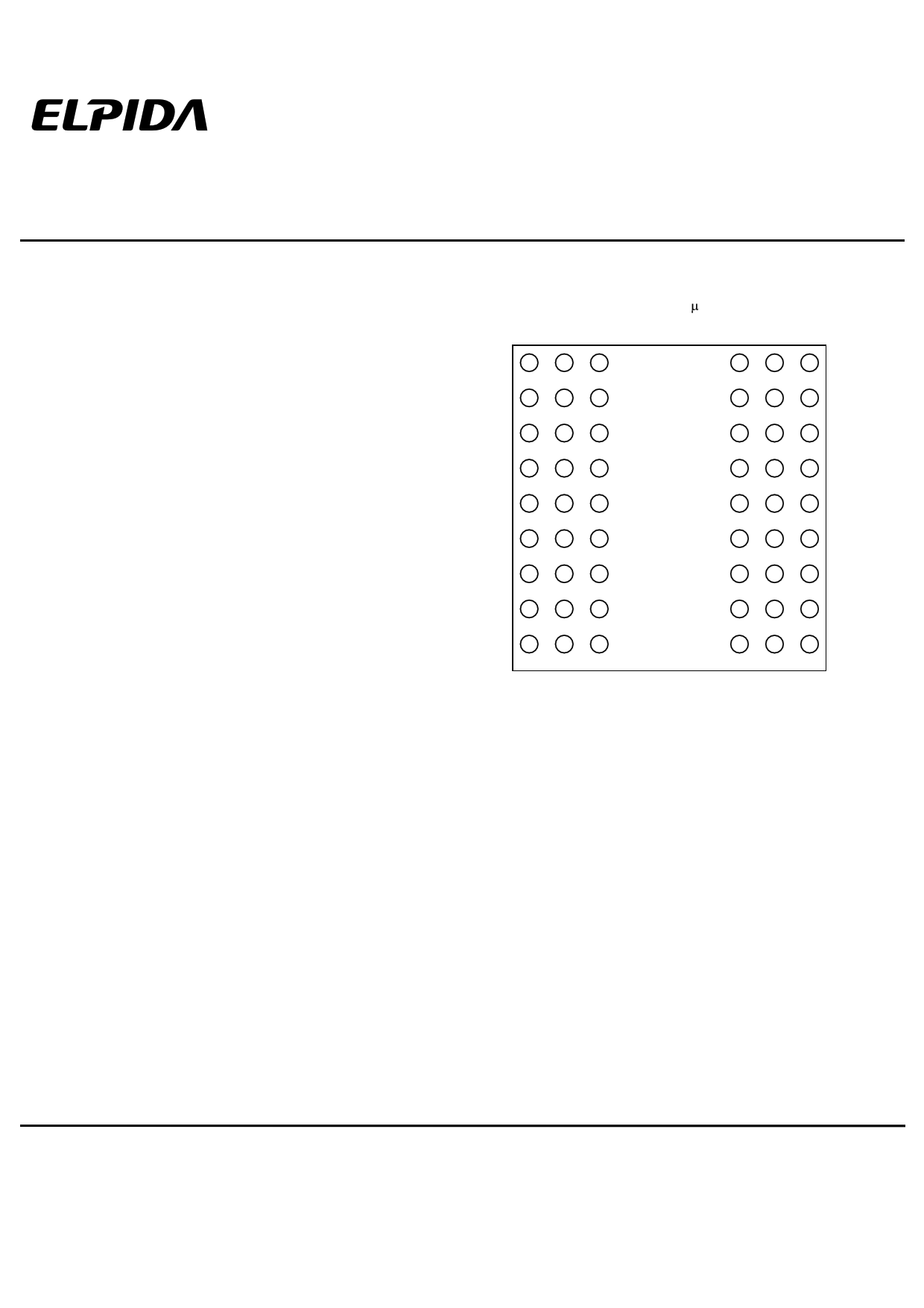
54-ball FBGA ( BGA)
123456789
A
VSS DQ15 VSSQ
B
DQ14 DQ13 VDDQ
C
DQ12 DQ11 VSSQ
D
DQ10 DQ9 VDDQ
E
DQ8 NC VSS
F
UDQM CLK CKE
G
NC A11 A9
H
A8 A7 A6
J
VSS A5 A4
VDDQ DQ0 VDD
VSSQ DQ2 DQ1
VDDQ DQ4 DQ3
VSSQ DQ6 DQ5
VDD LDQM DQ7
/CAS /RAS /WE
BA0 BA1 /CS
A0 A1 A10
A3 A2 VDD
(Top view)
A0 to A11
BA0, BA1
DQ0 to DQ15
CLK
CKE
/CS
/RAS
/CAS
/WE
UDQM
LDQM
VDD
VSS
VDDQ
VSSQ
NC
Address inputs
Bank select
Data inputs/ outputs
Clock input
Clock enable
Chip select
Row address strobe
Column address strobe
Write enable
Upper DQ mask enable
Lower DQ mask enable
Power supply
Ground
Power supply for DQ
Ground for DQ
No connection
Document No. E0195E30 (Ver. 3.0)
Date Published June 2002 (K) Japan
URL: http://www.elpida.com
Elpida Memory, Inc. 2001-2002
1 page 
EDL1216CASA
DC Characteristics 1 (TA = –25 to +85°C, VDD, VDDQ = 1.8V ± 0.15V, VSS, VSSQ = 0V)
Parameter
/CAS latency
Operating current
(CL = 2)
(CL = 3)
Standby current in power down
Standby current in power down
(input signal stable)
Symbol
IDD1
IDD1
IDD2P
IDD2PS
Standby current in non power
down
IDD2N
Standby current in non power
down (input signal stable)
Active standby current in power
down
Active standby current in power
down (input signal stable)
IDD2NS
IDD3P
IDD3PS
Active standby current in non
power down
IDD3N
Active standby current in non
power down (input signal stable)
IDD3NS
Burst operating current
(CL = 2)
IDD4
(CL = 3)
IDD4
Refresh current
(CL = 2)
IDD5
(CL = 3)
IDD5
Self refresh current
PASR="000" (Full)
IDD6
PASR="001" (2BK)
PASR="010" (1BK)
PASR="101" (1/2 BK)
PASR="110" (1/4 BK)
PASR="000" (Full)
IDD6
PASR="001" (2BK)
PASR="010" (1BK)
PASR="101" (1/2 BK)
PASR="110" (1/4 BK)
PASR="000" (Full)
IDD6
PASR="001" (2BK)
PASR="010" (1BK)
PASR="101" (1/2 BK)
PASR="110" (1/4 BK)
Standby current in deep power
down mode
IDD7
Grade max.
60
60
0.9
0.5
5.5
2
1.5
1
17
12
40
60
130
130
0.35
0.25
0.18
0.12
0.09
0.20
0.15
0.10
0.08
0.07
0.60
0.50
0.43
0.37
0.34
10
Unit Test condition
Notes
mA Burst length = 1
1
tRC ≥ tRC min., IO = 0mA,
mA One bank active
mA CKE ≤ VIL max., tCK = 15ns
mA CKE ≤ VIL max., tCK = ∞
CKE ≥ VIH min., tCK = 15ns,
mA
/CS ≥ VIH min.,
Input signals are changed one
time during 30ns.
mA
CKE ≥ VIH min., tCK = ∞,
Input signals are stable.
mA CKE ≤ VIL max., tCK = 15ns
mA CKE ≤ VIL max., tCK = ∞
CKE ≥ VIH min., tCK = 15 ns,
mA
/CS ≥ VIH min.,
Input signals are changed one
time during 30ns.
mA CKE ≥ VIH min., tCK = ∞,
Input signals are stable.
mA
tCK ≥ tCK min.,
IOUT = 0mA, All banks active
2
mA
mA tRC ≥ tRC min.
3
mA
mA TCSR="00" (Ts*4 ≤ 70°C)
mA CKE ≤ 0.2V
mA
mA
mA
mA TCSR="01" (Ts*4 ≤ 45°C)
mA CKE ≤ 0.2V
mA
mA
mA
mA TCSR="11" (Ts*4 ≤ 85°C)
mA CKE ≤ 0.2V
mA
mA
mA
µA CKE ≤ 0.2V
Data Sheet E0195E30 (Ver. 3.0)
5
5 Page 
EDL1216CASA
Precharge command (/CS, /RAS, /WE = Low, /CAS = High)
This command begins precharge operation of the bank selected by BA0 and BA1. When A10 is High, all banks are
precharged, regardless of BA0 and BA1. When A10 is Low, only the bank selected by BA0 and BA1 is precharged.
After this command, the Mobile RAM can’t accept the activate command to the precharging bank during tRP
(precharge to activate command period). This command corresponds to a conventional DRAM’s /RAS rising.
CLK
CKE
/CS
H
/RAS
/CAS
/WE
BA0, BA1
A10
(Precharge select)
Add
Precharge command
Write command (/CS, /CAS, /WE = Low, /RAS = High)
This command sets the burst start address given by the column address to begin the burst write operation. The first
write data in burst mode can input with this command with subsequent data on following clocks.
CLK
CKE
/CS
H
/RAS
/CAS
/WE
BA0, BA1
A10
Add Col.
Write command
Read command (/CS, /CAS = Low, /RAS, /WE = High)
Read data is available after /CAS latency requirements have been met. This command sets the burst start address
given by the column address.
CLK
CKE
/CS
H
/RAS
/CAS
/WE
BA0, BA1
A10
Add Col.
Read command
Data Sheet E0195E30 (Ver. 3.0)
11
11 Page | ||
| Páginas | Total 30 Páginas | |
| PDF Descargar | [ Datasheet EDL1216CASA.PDF ] | |
Hoja de datos destacado
| Número de pieza | Descripción | Fabricantes |
| EDL1216CASA | 128M bits Mobile RAM | Elpida Memory |
| Número de pieza | Descripción | Fabricantes |
| SLA6805M | High Voltage 3 phase Motor Driver IC. |
Sanken |
| SDC1742 | 12- and 14-Bit Hybrid Synchro / Resolver-to-Digital Converters. |
Analog Devices |
|
DataSheet.es es una pagina web que funciona como un repositorio de manuales o hoja de datos de muchos de los productos más populares, |
| DataSheet.es | 2020 | Privacy Policy | Contacto | Buscar |