|
|
|
PDF IDT72V265LA Data sheet ( Hoja de datos )
| Número de pieza | IDT72V265LA | |
| Descripción | 3.3 VOLT CMOS SuperSync FIFO 8/192 x 18 16/384 x 18 | |
| Fabricantes | Integrated Device Tech | |
| Logotipo | ||
Hay una vista previa y un enlace de descarga de IDT72V265LA (archivo pdf) en la parte inferior de esta página. Total 27 Páginas | ||
|
No Preview Available !
3.3 VOLT CMOS SuperSync FIFO™
8,192 x 18
16,384 x 18
IDT72V255LA
IDT72V265LA
FEATURES:
• Choose among the following memory organizations:
IDT72V255LA
8,192 x 18
IDT72V265LA
16,384 x 18
• Pin-compatible with the IDT72V275/72V285 and IDT72V295/
72V2105 SuperSync FIFOs
• Functionally compatible with the 5 Volt IDT72255/72265 family
• 10ns read/write cycle time (6.5ns access time)
• Fixed, low first word data latency time
• 5V input tolerant
• Auto power down minimizes standby power consumption
• Master Reset clears entire FIFO
• Partial Reset clears data, but retains programmable settings
• Retransmit operation with fixed, low first word data
latency time
• Empty, Full and Half-Full flags signal FIFO status
• Programmable Almost-Empty and Almost-Full flags, each flag
can default to one of two preselected offsets
• Program partial flags by either serial or parallel means
• Select IDT Standard timing (using EF and FF flags) or First
Word Fall Through timing (using OR and IR flags)
• Output enable puts data outputs into high impedance state
• Easily expandable in depth and width
• Independent Read and Write clocks (permit reading and
writing simultaneously)
• Available in the 64-pin Thin Quad Flat Pack (TQFP) and the 64-
pin Slim Thin Quad Flat Pack (STQFP)
• High-performance submicron CMOS technology
• Industrial temperature range (–40°C to +85°C) is available
DESCRIPTION:
The IDT72V255LA/72V265LA are functionally compatible versions of the
IDT72255/72265 designed to run off a 3.3V supply for very low power
consumption. The IDT72V255LA/72V265LA are exceptionally deep, high
speed, CMOS First-In-First-Out (FIFO) memories with clocked read and
write controls. These FIFOs offer numerous improvements over previous
SuperSync FIFOs, including the following:
• The limitation of the frequency of one clock input with respect to the other
has been removed. The Frequency Select pin (FS) has been removed,
thus it is no longer necessary to select which of the two clock inputs, RCLK
or WCLK, is running at the higher frequency.
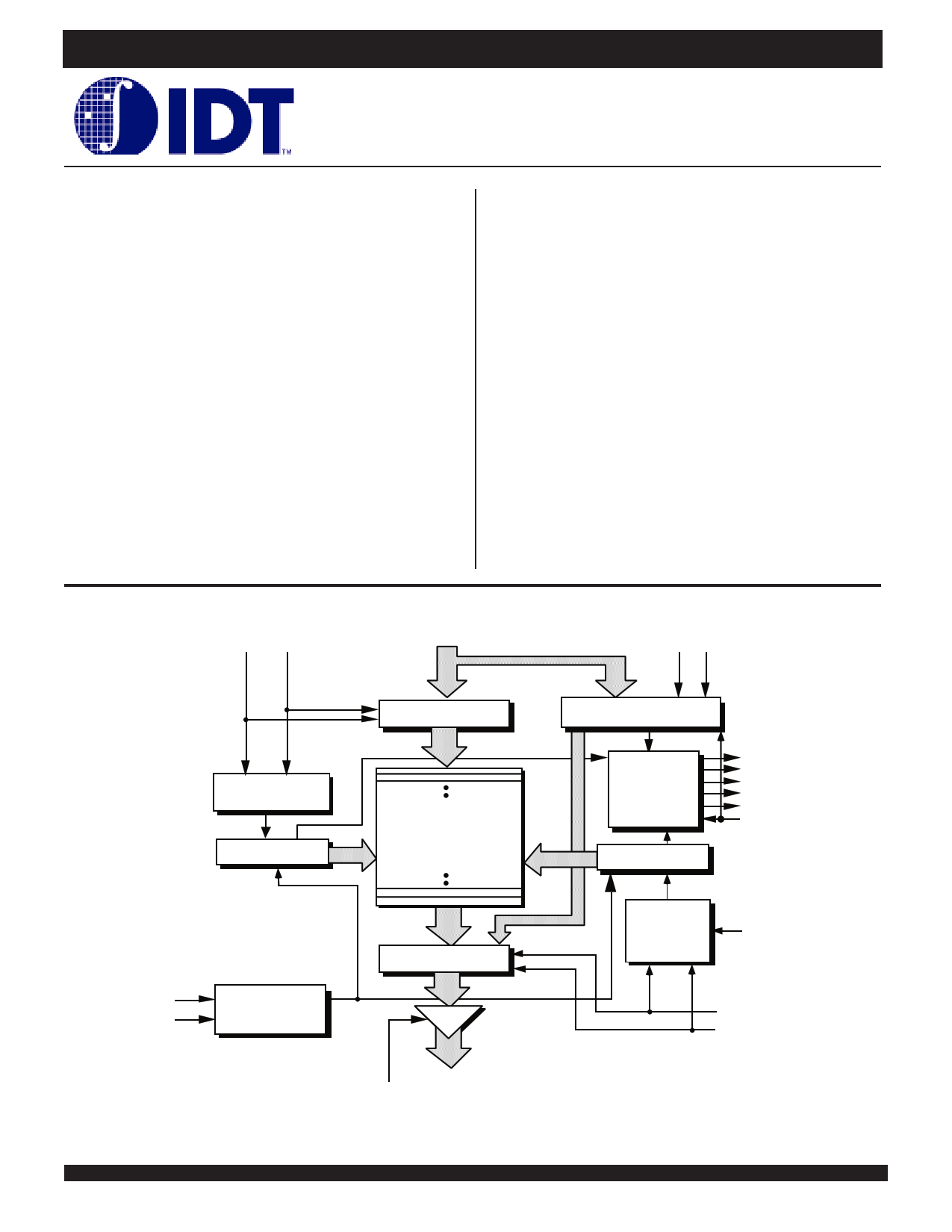
FUNCTIONAL BLOCK DIAGRAM
WEN WCLK
D0 -D17
LD SEN
WRITE CONTROL
LOGIC
WRITE POINTER
INPUT REGISTER
RAM ARRAY
8,192 x 18
16,384 x 18
OFFSET REGISTER
FLAG
LOGIC
READ POINTER
FF/IR
PAF
EF/OR
PAE
HF
FWFT/SI
MRS
PRS
RESET
LOGIC
OUTPUT REGISTER
READ
CONTROL
LOGIC
RT
RCLK
REN
Q0 -Q17
OE
The IDT logo is a registered trademark and the SuperSyncFIFO is a trademark of Integrated Device Technology, Inc.
COMMERCIAL AND INDUSTRIAL TEMPERATURE RANGES
1
© 2001 Integrated Device Technology, Inc
4672 drw 01
APRIL 2001
DSC-4672/1
1 page 
IDT72V255LA/72V265LA 3.3 VOLT CMOS SuperSync FIFO™
8,192 x 18, 16,384 x 18
COMMERCIAL AND INDUSTRIAL
TEMPERATURE RANGES
ABSOLUTE MAXIMUM RATINGS
Symbol
VTERM
TSTG
IOUT
Rating
Terminal Voltage
with respect to GND
Storage
Temperature
DC Output Current
Commercial
–0.5 to +5
–55 to +125
–50 to +50
Unit
V
°C
mA
NOTE:
1. Stresses greater than those listed under ABSOLUTE MAXIMUM RATINGS may cause
permanent damage to the device. This is a stress rating only and functional operation
of the device at these or any other conditions above those indicated in the operational
sections of this specification is not implied. Exposure to absolute maximum rating
conditions for extended periods may affect reliability.
RECOMMENDED DC OPERATING
CONDITIONS
Symbol
Parameter
Min. Typ. Max.
VCC Supply Voltage (Com’l/Ind’l)
3.0 3.3 3.6
GND Supply Voltage (Com’l/Ind’l)
0 00
VIH Input High Voltage (Com’l/Ind’l) 2.0 5.0
VIL(1) Input Low Voltage (Com’l/Ind’l) 0.8
TA Operating Temperature
Commercial
0 70
TA Operating Temperature
Industrial
0 85
NOTE:
1. 1.5V undershoots are allowed for 10ns once per cycle.
Unit
V
V
V
V
°C
°C
DC ELECTRICAL CHARACTERISTICS
(Commercial: VCC = 3.3V ± 0.3V, TA = 0°C to +70°C; Industrial: VCC = 3.3V ± 0.3V, TA = -40°C to +85°C)
IDT72V255LA
IDT72V265LA
Com’l & Ind’l(1)
tCLK = 10, 15, 20 ns
Symbol
ILI(2)
ILO(3)
Parameter
Input Leakage Current
Output Leakage Current
Min. Max.
–1 1
–10 10
VOH
VOL
ICC1(4,5,6)
Output Logic “1” Voltage, IOH = –2 mA
Output Logic “0” Voltage, IOL = 8 mA
Active Power Supply Current
2.4 —
— 0.4
— 55
ICC2(4,7)
Standby Current
— 20
NOTES:
1. Industrial temperature range product for 15ns speed grade is available as a standard device.
2. Measurements with 0.4 ≤ VIN ≤ VCC.
3. OE ≥ VIH, 0.4 ≤ VOUT ≤ VCC.
4. Tested with outputs disabled (IOUT = 0).
5. RCLK and WCLK toggle at 20 MHz and data inputs switch at 10 MHz.
6. Typical ICC1 = 10 + 1.1*fS + 0.02*CL*fS (in mA) with VCC = 3.3V, TA = 25°C, fS = WCLK frequency = RCLK frequency (in MHz, using TTL levels), data
switching at fS/2, CL = capacitive load (in pF).
7. All Inputs = VCC –0.2V or GND + 0.2V, except RCLK and WCLK, which toggle at 20 MHz.
Unit
µA
µA
V
V
mA
mA
CAPACITANCE
(TA = +25°C, f = 1.0MHz)
Symbol
CIN(2)
COUT(1,2)
Parameter(1)
Input
Capacitance
Output
Capacitance
Conditions
VIN = 0V
VOUT = 0V
NOTES:
1. With output deselected, (OE ≥ VIH).
2. Characterized values, not currently tested.
Max. Unit
10 pF
10 pF
5
5 Page 
IDT72V255LA/72V265LA 3.3 VOLT CMOS SuperSync FIFO™
8,192 x 18, 16,384 x 18
COMMERCIAL AND INDUSTRIAL
TEMPERATURE RANGES
If FWFT mode is selected, the FIFO will mark the beginning of the
Retransmit setup by setting OR HIGH. During this period, the internal read
pointer is set to the first location of the RAM array.
When OR goes LOW, Retransmit setup is complete; at the same time, the
contents of the first location appear on the outputs. Since FWFT mode is
selected, the first word appears on the outputs, no LOW on REN is
necessary. Reading all subsequent words requires a LOW on REN to
enable the rising edge of RCLK. See Figure 12, Retransmit Timing (FWFT
Mode), for the relevant timing diagram.
For either IDT Standard mode or FWFT mode, updating of the PAE, HF
and PAF flags begin with the rising edge of RCLK that RT is setup. PAE is
synchronized to RCLK, thus on the second rising edge of RCLK after RT is
setup, the PAE flag will be updated. HF is asynchronous, thus the rising
edge of RCLK that RT is setup will update HF. PAF is synchronized to
WCLK, thus the second rising edge of WCLK that occurs tSKEW after the
rising edge of RCLK that RT is setup will update PAF. RT is synchronized to
RCLK.
11
11 Page | ||
| Páginas | Total 27 Páginas | |
| PDF Descargar | [ Datasheet IDT72V265LA.PDF ] | |
Hoja de datos destacado
| Número de pieza | Descripción | Fabricantes |
| IDT72V265LA | 3.3 VOLT CMOS SuperSync FIFO 8/192 x 18 16/384 x 18 | Integrated Device Tech |
| Número de pieza | Descripción | Fabricantes |
| SLA6805M | High Voltage 3 phase Motor Driver IC. |
Sanken |
| SDC1742 | 12- and 14-Bit Hybrid Synchro / Resolver-to-Digital Converters. |
Analog Devices |
|
DataSheet.es es una pagina web que funciona como un repositorio de manuales o hoja de datos de muchos de los productos más populares, |
| DataSheet.es | 2020 | Privacy Policy | Contacto | Buscar |