|
|
PDF XRD98L59 Data sheet ( Hoja de datos )
| Número de pieza | XRD98L59 | |
| Descripción | CCD Image Digitizers with CDS/ PGA and 10-Bit A/D | |
| Fabricantes | Exar Corporation | |
| Logotipo |  |
|
Hay una vista previa y un enlace de descarga de XRD98L59 (archivo pdf) en la parte inferior de esta página. Total 30 Páginas | ||
|
No Preview Available !
XRD98L59
CCD Image Digitizers with
CDS, PGA and 10-Bit A/D
FEATURES
• 10-bit Resolution ADC
• 20MHz Sampling Rate
• Programmable Gain: 6dB to 38dB PGA
(2x to 80x)
• Improved Digitally Controlled Offset-Calibration
with Pixel Averager and Hot Pixel Clipper
• DNS Filter Removes Black Level Digital Noise
• Widest Black Level Calibration Range at
Maximum Gain
• Manual Control of Offset DAC via Serial Port for
Use with High Speed Scanners
• 2ns/step Programmable Aperture Delay on SPIX
and SBLK
• Single 2.7V to 3.6V Power Supply
•
Low Power for Battery Operation:120mW @ V =3V
DD
January 2001-2
• 5µA Typical Stand By Mode Current
• Three-State Digital Outputs
• 2,000V ESD Protection
• 28-pin TSSOP Package
APPLICATIONS
• Digital Still Cameras
• Digital Camcorders
• PC Video Cameras
• CCTV/Security Cameras
• Industrial/Medical Cameras
• 2D Bar Code Readers
• High Speed Scanners
• Digital Copiers
GENERAL DESCRIPTION
The XRD98L59 is a complete low power CCD Image
Digitizer for digital, motion and still cameras. The
product includes a high bandwidth differential Corre-
lated Double Sampler (CDS), 8-bit digitally Program-
mable Gain Amplifier (PGA), 10-bit Analog-to-Digital
Converter (ADC) and improved digitally controlled
black level auto-calibration circuitry with pixel averager
hot pixel clipper, and a DNS filter.
The Correlated Double Sampler (CDS) subtracts the
CCD output signal black level from the video level.
Common mode signal and power supply noise are
rejected by the differential CDS input stage.
The PGA is digitally controlled with 8-bit resolution on
a linear dB scale, resulting in a gain range of 6dB to
38dB with 0.125dB per LSB of the gain code.
The auto calibration circuit compensates for any inter-
nal offset of the XRD98L59 as well as black level offset
from the CCD.
The PGA and black level auto-calibration are con-
trolled through a simple 3-wire serial interface. The
timing circuitry is designed to enable users to select a
wide variety of available CCD and image sensors for
their applications.
The XRD98L59 has direct access to the ADC input for
digitizing other analog signals. The XRD98L59 is
packaged in 28-lead surface mount TSSOP to reduce
space and weight, and is suitable for hand-held and
portable applications.
ORDERING INFORMATION
Part No.
XRD98L59AIG
Package
28-Lead TSSOP
Operating
Maximum
Temperature Range Power Supply Sampling Rate
-40°C to 85°C
3.0V
20 MSPS
Rev. 2.00
EXAR Corporation, 48720 Kato Road, Fremont, CA 94538 • (510) 668-7000 • FAX (510) 668-7017 • www.exar.com
1 page 
XRD98L59
DC ELECTRICAL CHARACTERISTICS - XRD98L59 (CONT'D)
Unless otherwise specified: OVDD = DVDD = AVDD = 3.0V, Pixel Rate = 20MSPS, TA = 25°C
Symbol Parameter
Min. Typ. Max. Unit Conditions
System Specifications
DNLS
INLSMIN
System DNL
System INL @ Minimum Gain
-1 +0.75 1.5 LSB No missing codes, monotonic
2 LSB INL error is dominated by CDS/PGA
linearity
INLSMAX System INL @ Maximum Gain
2 LSB INL error is dominated by CDS/PGA
linearity
en MAXAV
Input Referred Noise @
Max Gain
0.2 mVrms Gain Code = FFh
en MINAV Input Referred Noise @
0.7 mVrms Gain Code = 00h
Min Gain
Latency Pipeline Delay
4 cycles
Digital Inputs
VIH Digital Input High Voltage
VIL Digital Input Low Voltage
IL DC Leakage Current
CIN Input Capacitance
Digital Outputs
2.1 V
0.5 V
5 µA VIN = GND or VDD
5 pF
VOH
VOL
IOZ
Digital Output High Voltage
Digital Output Low Voltage
High–Z Leakage
OVDD-0.5
-10
V
0.5 V
10 µA
While sourcing 2mA
While sinking 2mA
OE = 0 or PD = 1
Output = OGND or ODVDD
Rev. 2.00
5
5 Page 
XRD98L59
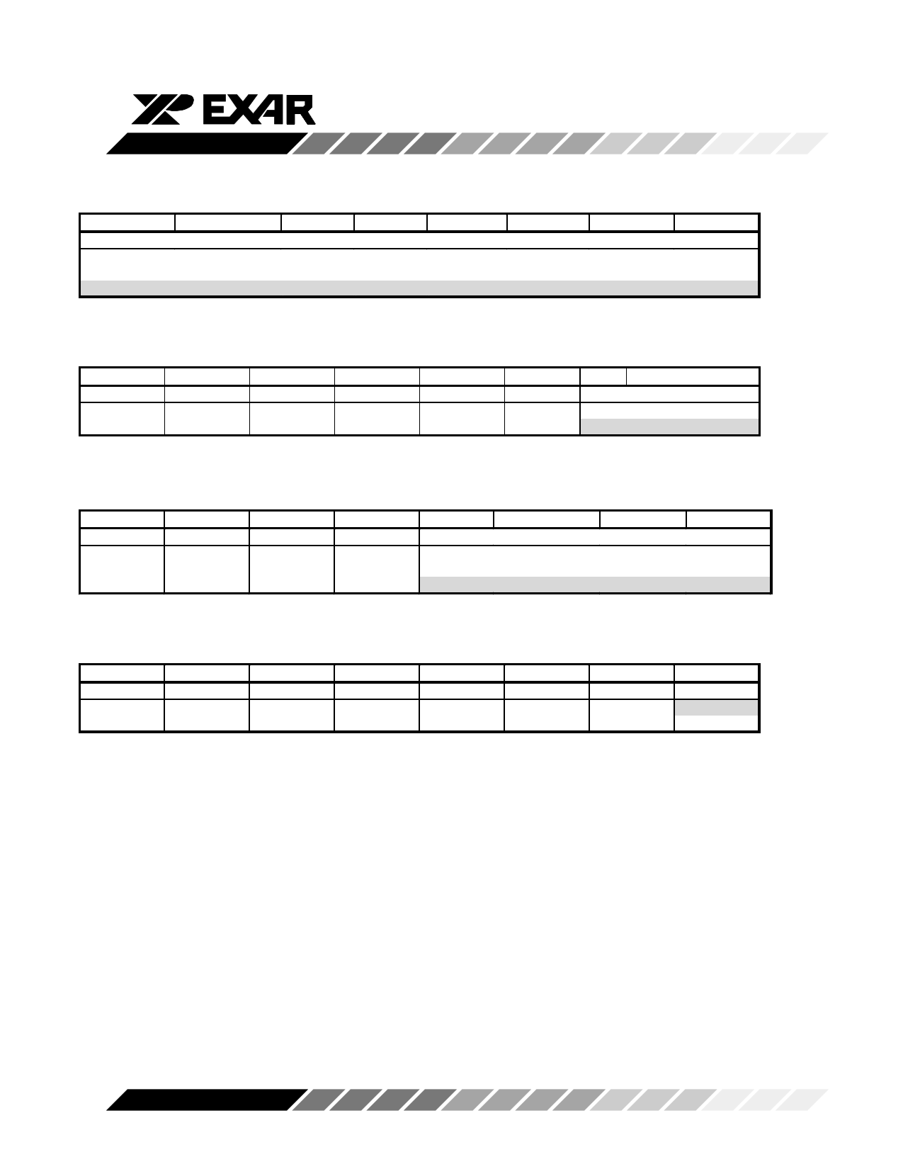
D7 D6
FDAC[9:2]
1 1 1 1 1 1 1 1 max pos offset
1 0 0 0 0 0 0 0 zero offset
0 0 0 0 0 0 0 0 max neg offset *
D5
D4
D3
D2
D1
Table 8. FDAC (MSB) Register bit assignment (Address 0110)
D0
D7
not used
D6
not used
D5
not used
D4
not used
D3
not used
D2
not used
D1
11
00
D0
FDAC[1:0]
max pos offset
max neg offset *
Table 9. FDAC (LSB) Register bit assignment (Address 0111)
D7
not used
D6
not used
D5
not used
D4
not used
D3
1111
1011
0000
D2 D1
CDAC[3:0]
max pos offset +50 mV
zero offset
max neg offset * -137.5 mV
Table 10. CDAC Register bit assignment (Address 1000)
D0
D7
not used
D6
not used
D5
not used
D4
not used
D3
not used
D2
not used
D1
not used
D0
Reset
0 normal *
1 reset chip
Table 11. Reset Register bit assignment (Address 1111)
Note: * Shading indicates default values after power up or reset. The XRD98L59 does not reset the
registers to default value after PD.
Rev. 2.00
11
11 Page | ||
| Páginas | Total 30 Páginas | |
| PDF Descargar | [ Datasheet XRD98L59.PDF ] | |
Hoja de datos destacado
| Número de pieza | Descripción | Fabricantes |
| XRD98L53 | CCD Image Digitizers | Exar Corporation |
| XRD98L59 | CCD Image Digitizers with CDS/ PGA and 10-Bit A/D | Exar Corporation |
| Número de pieza | Descripción | Fabricantes |
| SLA6805M | High Voltage 3 phase Motor Driver IC. |
Sanken |
| SDC1742 | 12- and 14-Bit Hybrid Synchro / Resolver-to-Digital Converters. |
Analog Devices |
|
DataSheet.es es una pagina web que funciona como un repositorio de manuales o hoja de datos de muchos de los productos más populares, |
| DataSheet.es | 2020 | Privacy Policy | Contacto | Buscar |
