|
|
|
PDF AD9884A Data sheet ( Hoja de datos )
| Número de pieza | AD9884A | |
| Descripción | 100 MSPS/140 MSPS Analog Flat Panel Interface | |
| Fabricantes | Analog Devices | |
| Logotipo | ||
Hay una vista previa y un enlace de descarga de AD9884A (archivo pdf) en la parte inferior de esta página. Total 25 Páginas | ||
|
No Preview Available !
a
FEATURES
140 MSPS Maximum Conversion Rate
500 MHz Analog Bandwidth
0.5 V to 1.0 V Analog Input Range
400 ps p-p PLL Clock Jitter
Power-Down Mode
3.3 V Power Supply
2.5 V to 3.3 V Three-State CMOS Outputs
Demultiplexed Output Ports
Data Clock Output Provided
Low Power: 570 mW Typical
Internal PLL Generates CLOCK from HSYNC
Serial Port Interface
Fully Programmable
Supports Alternate Pixel Sampling for Higher-
Resolution Applications
APPLICATIONS
RGB Graphics Processing
LCD Monitors and Projectors
Plasma Display Panels
Scan Converters
100 MSPS/140 MSPS
Analog Flat Panel Interface
AD9884A
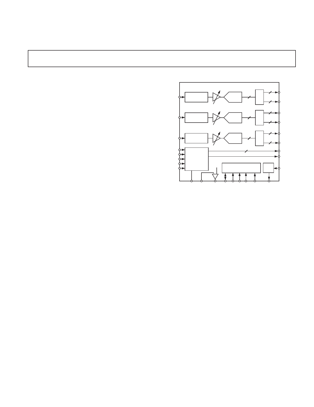
FUNCTIONAL BLOCK DIAGRAM
RIN CLAMP
GIN CLAMP
BIN CLAMP
HSYNC
COAST
CLAMP
CKINV
CKEXT
CLOCK
GENERATOR
0.15V
8
A/D
8
A/D
8
A/D
2
AD9884A
8
8
ROUTA
ROUTB
8
GOUTA
8
GOUTB
8
BOUTA
8
BOUTB
DATACK
HSOUT
CONTROL
REF
REFIN
FILT SOGIN SOGOUT SDA SCL A0 A1 PWRDN REFOUT
GENERAL DESCRIPTION
The AD9884A is a complete 8-bit 140 MSPS monolithic analog
interface optimized for capturing RGB graphics signals from
personal computers and workstations. Its 140 MSPS encode
rate capability and full-power analog bandwidth of 500 MHz
supports display resolutions of up to 1280 × 1024 (SXGA) at
75 Hz with sufficient input bandwidth to accurately acquire and
digitize each pixel.
To minimize system cost and power dissipation, the AD9884A
includes an internal 1.25 V reference, PLL to generate a pixel
clock from HSYNC, and programmable gain, offset and clamp
circuits. The user provides only a 3.3 V power supply, analog
input, and HSYNC signals. Three-state CMOS outputs may be
powered by a supply between 2.5 V and 3.3 V.
The AD9884A’s on-chip PLL generates a pixel clock from the
HSYNC input. Pixel clock output frequencies range from
20 MHz to 140 MHz. PLL clock jitter is typically 400 ps p-p
relative to the input reference. When the COAST signal is pre-
sented, the PLL maintains its output frequency in the absence
of HSYNC. A 32-step sampling phase adjustment is provided.
Data, HSYNC and Data Clock output phase relationships are
always maintained. The PLL can be disabled and an external
clock input provided as the pixel clock.
A clamp signal is generated internally or may be provided by the
user through the CLAMP input pin. This device is fully program-
mable via a two-wire serial port.
Fabricated in an advanced CMOS process, the AD9884A is
provided in a space-saving 128-lead MQFP surface mount plastic
package and is specified over a 0°C to +70°C temperature range.
REV. C
Information furnished by Analog Devices is believed to be accurate and
reliable. However, no responsibility is assumed by Analog Devices for its
use, nor for any infringements of patents or other rights of third parties that
may result from its use. No license is granted by implication or otherwise
under any patent or patent rights of Analog Devices.
One Technology Way, P.O. Box 9106, Norwood, MA 02062-9106, U.S.A.
Tel: 781/329-4700
www.analog.com
Fax: 781/326-8703
© Analog Devices, Inc., 2001
1 page 
AD9884A
Table I. Package Interconnections
Signal Type Name
Inputs
RAIN
GAIN
BAIN
HSYNC
COAST
CLAMP
SOGIN
CKEXT
CKINV
Outputs
DRA7-0
DRB7-0
DGA7-0
DGB7-0
DBA7-0
DBB7-0
DATACK
DATACK
HSOUT
SOGOUT
Control
SDA
SCL
A0, A1
PWRDN
Analog Interface REFOUT
REFIN
FILT
Power Supply VD
VDD
PVD
GND
No Connect NC
Function
Value
Package Pin
Analog Input for RED Channel
Analog Input for GREEN Channel
Analog Input for BLUE Channel
0.5 V to 1.0 V FS
0.5 V to 1.0 V FS
0.5 V to 1.0 V FS
7
15
22
Horizontal Sync Input
3.3 V CMOS
Clock Generator Coast Input (Optional) 3.3 V CMOS
External Clamp Input (Optional)
3.3 V CMOS
Sync On Green Slicer Input (Optional) 0.5 V to 1.0 V FS
40
41
28
14
External Clock Input (Optional)
Sampling Clock Inversion (Optional)
3.3 V CMOS
3.3 V CMOS
44
27
Data Output, Red Channel, Port A
Data Output, Red Channel, Port B
Data Output, Green Channel, Port A
Data Output, Green Channel, Port B
Data Output, Blue Channel, Port A
Data Output, Blue Channel, Port B
3.3 V CMOS
3.3 V CMOS
3.3 V CMOS
3.3 V CMOS
3.3 V CMOS
3.3 V CMOS
105–112
95–102
85–92
75–82
65–72
55–62
Data Output Clock
Data Output Clock Complement
3.3 V CMOS
3.3 V CMOS
115
116
Horizontal Sync Output
Sync On Green Slicer Output
3.3 V CMOS
3.3 V CMOS
117
118
Serial Data I/O
Serial Interface Clock
Serial Port Address LSBs
3.3 V CMOS
3.3 V CMOS
3.3 V CMOS
29
30
31, 32
Power-Down Control Input
3.3 V CMOS
125
Internal Reference Output
Reference Input
External Filter Connection
1.25 V
1.25 V ± 10%
126
127
45
Main Power Supply
Digital Output Power Supply
Clock Generator Power Supply
Ground
3.3 V ± 10%
2.5 V to 3.3 V ± 10%
3.3 V ± 10%
0V
4, 8, 10, 11, 16, 18, 19, 23, 25,
124, 128
54, 64, 74, 84, 94, 104, 114, 120
33, 34, 43, 48, 50
5, 6, 9, 12, 13, 17, 20, 21, 24, 26,
35, 39, 42, 47, 49, 51, 52, 53, 63,
73, 83, 93, 103, 113, 119, 121,
122, 123
1–3, 36–38, 46
–4– REV. C
5 Page 
AD9884A
INPUT GAIN
02 7–0 REDGAIN Red Channel Gain Adjust
An 8-bit word that sets the gain of the RED channel. The
AD9884A can accommodate input signals with a full-scale
range of between 0.5 V and 1.0 V p-p. Setting REDGAIN to
255 corresponds to an input range of 1.0 V. A REDGAIN of
0 establishes an input range of 0.5 V. Note that increasing
REDGAIN results in the picture having less contrast (the
input signal uses fewer of the available converter codes). See
Figure 8.
The power-up default value is REDGAIN = 80h.
03 7–0 GRNGAIN Green Channel Gain Adjust
An 8-bit word that sets the gain of the GREEN channel. See
REDGAIN (02).
The power-up default value is GRNGAIN = 80h.
04 7–0 BLUGAIN Blue Channel Gain Adjust
An 8-bit word that sets the gain of the BLUE channel. See
REDGAIN (02).
The power-up default value is BLUGAIN = 80h.
INPUT OFFSET
05 7–2 REDOFST Red Channel Offset Adjust
A six-bit offset binary word that sets the dc offset of the RED
channel.
One LSB of offset adjustment equals approximately one LSB
change in the ADC offset. Therefore, the absolute magnitude of
the offset adjustment scales as the gain of the channel is changed
(Figure 9). A nominal setting of 31 results in the channel nomi-
nally clamping the back porch (during the clamping interval) to
code 00. An offset setting of 63 results in the channel clamping
to code 31 of the ADC. An offset setting of 0 clamps to code
–31 (off the bottom of the range). Increasing the value of
REDOFST decreases the brightness of the channel.
The power-up default value is REDOFST = 80h.
06 7–2 GRNOFST Green Channel Offset Adjust
A six-bit offset binary word that sets the dc offset of the GREEN
channel. See REDOFST (05).
The power-up default value is GRNOFST = 80h.
07 7–2 BLUOFST Blue Channel Offset Adjust
A six-bit offset binary word that sets the DC offset of the GREEN
channel. See REDOFST (05).
The power-up default value is BLUOFST = 80h.
CLAMP TIMING
08 7–0
CLPLACE
Clamp Placement
An 8-bit register that sets the position of the internally generated clamp.
When EXTCLMP = 0, a clamp signal is generated internally, at
a position established by CLPLACE and for a duration set by
CLDUR. Clamping is started CLPLACE pixel periods after the
trailing edge of HSYNC. CLPLACE may be programmed to
any value between 1 and 255. CLPLACE = 0 is not supported.
The clamp should be placed during a time that the input signal
presents a stable black-level reference, usually the back porch
period between HSYNC and the image. A value of 08h will
usually work.
When EXTCLMP = 1, this register is ignored.
The power-up default value is CLPLACE = 80h.
09 7–0
CLDUR
Clamp Duration
An 8-bit register that sets the duration of the internally gener-
ated clamp.
When EXTCLMP = 0, a clamp signal is generated internally, at
a position established by CLPLACE and for a duration set by
CLDUR. Clamping is started CLPLACE pixel periods after the
trailing edge of HSYNC, and continues for CLDUR pixel peri-
ods. CLDUR may be programmed to any value between 1 and
255. CLDUR = 0 is not supported.
For the best results, the clamp duration should be set to include
the majority of the black reference signal time found following
the HSYNC signal trailing edge. Insufficient clamping time can
produce brightness changes at the top of the screen, and a slow
recovery from large changes in the Average Picture Level (APL), or
brightness. A value of 10h to 20h works with most standard signals.
When EXTCLMP = 1, this register is ignored.
The power-up default value is CLDUR = 80h.
–10–
REV. C
11 Page | ||
| Páginas | Total 25 Páginas | |
| PDF Descargar | [ Datasheet AD9884A.PDF ] | |
Hoja de datos destacado
| Número de pieza | Descripción | Fabricantes |
| AD9884A | 100 MSPS/140 MSPS Analog Flat Panel Interface | Analog Devices |
| Número de pieza | Descripción | Fabricantes |
| SLA6805M | High Voltage 3 phase Motor Driver IC. |
Sanken |
| SDC1742 | 12- and 14-Bit Hybrid Synchro / Resolver-to-Digital Converters. |
Analog Devices |
|
DataSheet.es es una pagina web que funciona como un repositorio de manuales o hoja de datos de muchos de los productos más populares, |
| DataSheet.es | 2020 | Privacy Policy | Contacto | Buscar |