|
|
|
PDF ADV7802 Data sheet ( Hoja de datos )
| Número de pieza | ADV7802 | |
| Descripción | SDTV/HDTV 3D Comb Filter & Video Decoder and Graphics Digitizer | |
| Fabricantes | Analog Devices | |
| Logotipo | ||
Hay una vista previa y un enlace de descarga de ADV7802 (archivo pdf) en la parte inferior de esta página. Total 30 Páginas | ||
|
No Preview Available !
Data Sheet
12-Bit, SDTV/HDTV 3D Comb Filter,
Video Decoder, and Graphics Digitizer
ADV7802
FEATURES
4 noise shaped video (NSV) 12-bit ADCs
True 12-bit high dynamic range processing
12-channel analog input mux
36-bit digital YCrCb/RGB output
12-bit deep color processing
Analog monitor output
NTSC/PAL/SECAM color standards support
NTSC/PAL 3D comb filter
3D digital noise reduction (DNR)
Advanced time-base correction (TBC) with frame
synchronization
Interlaced-to-progressive conversion for 525i and 625i
Advanced VBI data slicer, including teletext, CC, and V-chip
IF compensation filter
SCART fast blank support including slow switch detect
Programmable internal antialias filters
Weak, poor time-base, and nonstandard signal support
Vertical peaking, horizontal peaking, CTI, LTI
Simultaneous interlaced and progressive parallel output for
525i/525p and 625i/625p
525p/625p component progressive scan support
720p/1080i/1080p component HDTV support
Digitizes RGB graphics with maximum pixel clock rate of
135 MHz (ADV7802BSTZ-150 model only)
24-bit digital input port supports data from DVI/HDMI Rx IC
Any-to-any, advanced 3 × 3 color space conversion matrix
Flexible output pixel interface supporting 8-/10-/12-/16-/
20-/24-/30-/36-bit SDR/DDR 4:2:2/4:4:4 data formats
Programmable interrupt request output pin
APPLICATIONS
AV receivers
LCD HDTVs
PDP HDTVs
CRT HDTVs
HDTV STBs with PVR
DVD recorders with progressive scan input support
Projectors
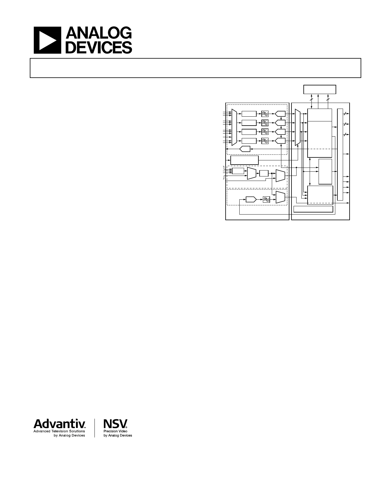
ADV7802
GR RGB
ANALOG INPUT INTERFACE
CLAMP
ADC
YPrPb
CLAMP
ADC
SCART
CVBS
S-VIDEO
HS_IN1
VS_IN1
SOG
XTAL
CLAMP
ADC
CLAMP
ADC
DAC
DIGITAL INPUT
INTERFACE
ADC_CLK
SYNC
CP
SDP
PLL
ADC, CORE, MEMORY
CLK GENERATION
DDS FOR SDP LINE-LOCKED
CLK GENERATION
DAC
ANA
DIG
CP
SDP
ANALOG
DDR/SDR SDRAM
INTERFACE
DATA (16)
CLK
ADDRESS (14)
CONTROL (9)
DDR/SDR
SDRAM
INTERFACE
STANDARD
DEFINITION
PROCESSOR
(SDP)
12
Y
12
Cb
12
Cr
CORE_CLK
CORE_CLK
COMPONENT
PROCESSOR
(CP)
I2C CONFIGURATION
DIGITAL
HS
VS
FLD
DE
LLC
Figure 1. ADV7802 Block Diagram
GENERAL DESCRIPTION
The ADV78021 is a high quality, single-chip, multiformat 3D comb
filter, video decoder, and graphics digitizer. This multiformat 3D
comb filter decoder supports the conversion of PAL, NTSC, and
SECAM standards in the form of a composite or an S-video into
a digital ITU-R BT.656 format. The ADV7802 also supports the
decoding of a component RGB/YPrPb video signal into a digital
YCrCb or RGB pixel output stream.
The support for component video includes standards such as 525i,
625i, 525p, 625p, 720p, 1080i, 1080p, and many other HD and
SMPTE standards. Graphics digitization is supported by the
ADV7802; it is capable of digitizing RGB graphics signals from
VGA to SXGA rates and converting them into a digital RGB or
YCrCb pixel output stream. SCART and overlay functionality are
enabled by the ability of the ADV7802 to simultaneously process
CVBS and standard definition RGB signals.
The ADV7802 contains two main processing sections. The first
section is the standard definition processor (SDP), which
processes all PAL, NTSC, SECAM, and component (up to
525p/625p) signal types. The second section is the component
processor (CP), which processes YPrPb and RGB component
formats, including RGB graphics.
1 Protected by U.S. Patent Number 4,907,093 and other intellectual
property rights.
Rev. D
Information furnished by Analog Devices is believed to be accurate and reliable. However, no
responsibility is assumed by Analog Devices for its use, nor for any infringements of patents or other
rights of third parties that may result from its use. Specifications subject to change without notice. No
license is granted by implication or otherwise under any patent or patent rights of Analog Devices.
Trademarksandregisteredtrademarksarethepropertyoftheirrespectiveowners.
One Technology Way, P.O. Box 9106, Norwood, MA 02062-9106, U.S.A.
Tel: 781.329.4700
www.analog.com
Fax: 781.461.3113
©2011 Analog Devices, Inc. All rights reserved.
1 page 
ADV7802
Data Sheet
SPECIFICATIONS
ELECTRICAL CHARACTERISTICS
AVDD = 3.15 V to 3.45 V, DVDD = 1.75 V to 1.85 V, DVDDIO = 3.0 V to 3.6 V, DVDDIO_SDRAM = 2.35 V to 2.65 V (DDR),
DVDDIO_SDRAM = 3.2 V to 3.4 V (SDR), PVDD = 1.71 V to 1.89 V, nominal input range 1.6 V. TA = 0°C to 85°C, unless
otherwise noted.
Table 1.
Parameter1
STATIC PERFORMANCE2, 3
Resolution (Each ADC)
Integral Nonlinearity4
Differential Nonlinearity4
POWER REQUIREMENTS5
Digital Core Power Supply
Digital I/O Power Supply
PLL Power Supply
Analog Power Supply
Memory Interface Power Supply
Digital Core Supply Current
Digital I/O Supply Current
PLL Supply Current
Analog Supply Current
Memory Interface Supply Current
Power-Down Current
Power-Up Time
DIGITAL INPUTS
Input High Voltage
Input Low Voltage
Input Current
Input Capacitance
Symbol
N
INL
DNL
DVDD
DVDDIO
PVDD
AVDD
DVDDIO_SDRAM
IDVDD
IDVDDIO
IPVDD
IAVDD
IVDDRAM
IPWRDN
tPWRUP
VIH
VIL
IIN
CIN
Test Conditions
BSL at 27 MHz (at a 12-bit level)
BSL at 54 MHz (at a 12-bit level)
BSL at 74 MHz (at an 11-bit level)
BSL at 110 MHz (at a 10-bit level)
BSL at 150 MHz (at an 8-bit level)
At 27 MHz (at a 12-bit level)
At 54 MHz (at a 12-bit level)
At 74 MHz (at an 11-bit level)
At 110 MHz (at a 10-bit level)
At 150 MHz (at an 8-bit level)
DDR
SDR
CVBS input sampling at 54 MHz
Graphics RGB sampling at 78 MHz
SCART RGB FB sampling at 54 MHz
525p input sampling at 54 MHz
Graphics RGB sampling at 135 MHz
1080p sampling at 148.5 MHz
CVBS input sampling at 54 MHz
Graphics RGB sampling at 78 MHz
Graphics RGB sampling at 135 MHz
1080p sampling at 148.5 MHz
CVBS input sampling at 54 MHz
Graphics RGB sampling at 78 MHz
Graphics RGB sampling at 135 MHz
1080p sampling at 148.5 MHz
CVBS input sampling at 54 MHz
SCART RGB FB sampling at 54 MHz
Graphics RGB sampling at 78 MHz
Graphics RGB sampling at 135 MHz
1080p sampling at 148.5 MHz
CVBS input sampling at 54 MHz
Min Typ
Max
−1.0/+1.5
−1.5/+2.0
−1.4/+1.2
−0.8/+2.0
−2.0/+2.0
−0.6/+0.7
−0.6/+0.8
−0.9/+0.75
−0.5/+1.0
−0.7/+1.5
12
1.75 1.8
3.0 3.3
1.71 1.8
3.15 3.3
2.35 2.5
3.2 3.3
236
103
236
319
180
214
6
15
27
48
13
10
10
11
99
269
263
286
288
17
8
20
1.85
3.6
1.89
3.45
2.65
3.4
2
0.8
±10
15
Unit
Bits
LSB
LSB
LSB
LSB
LSB
LSB
LSB
LSB
LSB
LSB
V
V
V
V
V
V
mA
mA
mA
mA
mA
mA
mA
mA
mA
mA
mA
mA
mA
mA
mA
mA
mA
mA
mA
mA
mA
ms
V
V
µA
pF
Rev. D | Page 4 of 36
5 Page 
ADV7802
ABSOLUTE MAXIMUM RATINGS
Table 5.
Parameter
AVDD to AGND
DVDD to DGND
PVDD to AGND
DVDDIO to DGND
DVDDIO_SDRAM to
DGND_SDRAM (DDR)
DVDDIO_SDRAM to
DGND_SDRAM (SDR)
DVDDIO to AVDD
DVDDIO to DVDD
DVDDIO_SDRAM to DVDD (DDR)
DVDDIO_SDRAM to DVDD (SDR)
AVDD to PVDD
AVDD to DVDD
DVDDIO to DVDDIO_SDRAM (DDR)
DVDDIO to DVDDIO_SDRAM (SDR)
AVDD to DVDDIO_SDRAM (DDR)
AVDD to DVDDIO_SDRAM (SDR)
Digital Inputs Voltage to DGND
DVDDIO_SDRAM Inputs to
DGND_SDRAM
Analog Inputs to AGND
SCLK/SDA Data Pins to DVDDIO
Maximum Junction Temperature
(TJ MAX)
Storage Temperature Range
Infrared Reflow Soldering (20 sec)
Rating
4.0 V
2.2 V
2.2 V
4.0 V
2.7 V
4.0 V
−0.3 V to +0.3 V
−0.3 V to +2 V
−0.3 V to +2.5 V
−0.3 V to +3.3 V
−0.3 V to +2 V
−0.3 V to +2 V
−0.3 V to +2 V
−0.3 V to +3.3 V
−0.3 V to +2.5 V
−0.3 V to +1.8 V
DGND − 0.3 V to DVDDIO + 0.3 V
DGND_SDRAM − 0.3 V to
DVDDIO_SDRAM + 0.3 V
AGND − 0.3 V to AVDD + 0.3 V
DVDDIO − 0.3 V to DVDDIO + 3.6 V
125°C
−65°C to +150°C
260°C
Stresses above those listed under Absolute Maximum Ratings
may cause permanent damage to the device. This is a stress
rating only; functional operation of the device at these or any
other conditions above those indicated in the operational
section of this specification is not implied. Exposure to absolute
maximum rating conditions for extended periods may affect
device reliability.
Data Sheet
PACKAGE THERMAL PERFORMANCE
To reduce power consumption when using the part, the user is
advised to turn off any unused ADCs.
The junction temperature must always stay below the
maximum junction temperature (TJ MAX) of 125°C. The
following equation shows how to calculate the junction
temperature:
TJ = TA MAX + (θJA × WMAX)
where:
TA MAX = 85°C.
θJA = 21.0330°C/W.
WMAX = ((AVDD × IAVDD) + (DVDD × IDVDD) + (DVDDIO ×
IDVDDIO) + (PVDD × IPVDD) + (DVDDIO_SDRAM ×
DVDDIO_SDRAM)).
THERMAL RESISTANCE
θJA is specified for the worst-case conditions, that is, a device
soldered in a circuit board for surface-mount packages.
Table 6. Thermal Resistance
Package Type
θJA1 θJC2 Unit
176-Lead LQFP
21 7
°C/W
1 4-layer PCB with solid ground plane.
2 4-layer PCB with solid ground plane (still air).
ESD CAUTION
Rev. D | Page 10 of 36
11 Page | ||
| Páginas | Total 30 Páginas | |
| PDF Descargar | [ Datasheet ADV7802.PDF ] | |
Hoja de datos destacado
| Número de pieza | Descripción | Fabricantes |
| ADV7800 | SDTV/HDTV 3D Comb Filter & Video Decoder and Graphics Digitizer | Analog Devices |
| ADV7802 | SDTV/HDTV 3D Comb Filter & Video Decoder and Graphics Digitizer | Analog Devices |
| Número de pieza | Descripción | Fabricantes |
| SLA6805M | High Voltage 3 phase Motor Driver IC. |
Sanken |
| SDC1742 | 12- and 14-Bit Hybrid Synchro / Resolver-to-Digital Converters. |
Analog Devices |
|
DataSheet.es es una pagina web que funciona como un repositorio de manuales o hoja de datos de muchos de los productos más populares, |
| DataSheet.es | 2020 | Privacy Policy | Contacto | Buscar |