|
|
|
PDF ADP5133 Data sheet ( Hoja de datos )
| Número de pieza | ADP5133 | |
| Descripción | 800 mA Buck Regulators | |
| Fabricantes | Analog Devices | |
| Logotipo | ||
Hay una vista previa y un enlace de descarga de ADP5133 (archivo pdf) en la parte inferior de esta página. Total 25 Páginas | ||
|
No Preview Available !
Data Sheet
Dual 3 MHz, 800 mA Buck Regulators in WLCSP
ADP5133
FEATURES
Input voltage range: 2.3 V to 5.5 V
Two 800 mA buck regulators
Tiny, 16-ball, 2 mm × 2 mm WLCSP package
Regulator accuracy: ±1.8%
Factory programmable or external adjustable VOUTx
3 MHz buck operation with forced PWM and auto PWM/PSM
modes
BUCK1/BUCK2: output voltage range from 0.8 V to 3.8 V
APPLICATIONS
Power for processors, ASICs, FPGAs, and RF chipsets
Portable instrumentation and medical devices
Space constrained devices
GENERAL DESCRIPTION
The ADP5133 combines two high performance buck regulators
in a tiny, 16-ball, 2 mm × 2 mm WLCSP to meet demanding
performance and board space requirements.
The high switching frequency of the buck regulators enables tiny
multilayer external components and minimizes the board space.
When the MODE pin is set high, the buck regulators operate in
forced PWM mode. When the MODE pin is set low and the
buck regulators operate in PWM mode, the load current is above
a predefined threshold. When the load current falls below a
predefined threshold, the regulators operate in power save
mode (PSM), improving the light load efficiency.
The two bucks operate out of phase to reduce the input capacitor
requirement and noise.
The regulators in the ADP5133 are activated through dedicated
enable pins. The output voltages can be externally set through a
resistor feedback network.
Table 1. Related Devices
Model
ADP5023
ADP5024
ADP5034
Channels
2 Bucks, 1 LDO
2 Bucks, 1 LDO
2 Bucks, 2 LDOs
ADP5037
ADP5033
ADP5040
ADP5041
ADP5133
ADP5134
2 Bucks, 2 LDOs
2 Bucks, 2 LDOs with
2 ENx pins
1 Buck, 2 LDOs
1 Buck, 2 LDOs with
supervisory, watchdog,
manual reset
2 Bucks with 2 ENx pins
2 Bucks, 2 LDOs with
precision enable and
power-good output
Maximum
Current
800 mA, 300 mA
1.2 A, 300 mA
1.2 A, 300 mA
800 mA, 300 mA
800 mA, 300 mA
1.2 A, 300 mA
1.2 A, 300 mA
800 mA
1.2 A, 300 mA
Package
LFCSP (CP-24-10)
LFCSP (CP-24-10)
LFCSP (CP-24-10),
TSSOP (RE-28-1)
LFCSP (CP-24-10)
WLCSP (CB-16-8)
LFCSP (CP-20-10)
LFCSP (CP-20-10)
WLCSP (CB-16-8)
LFCSP (CP-24-7)
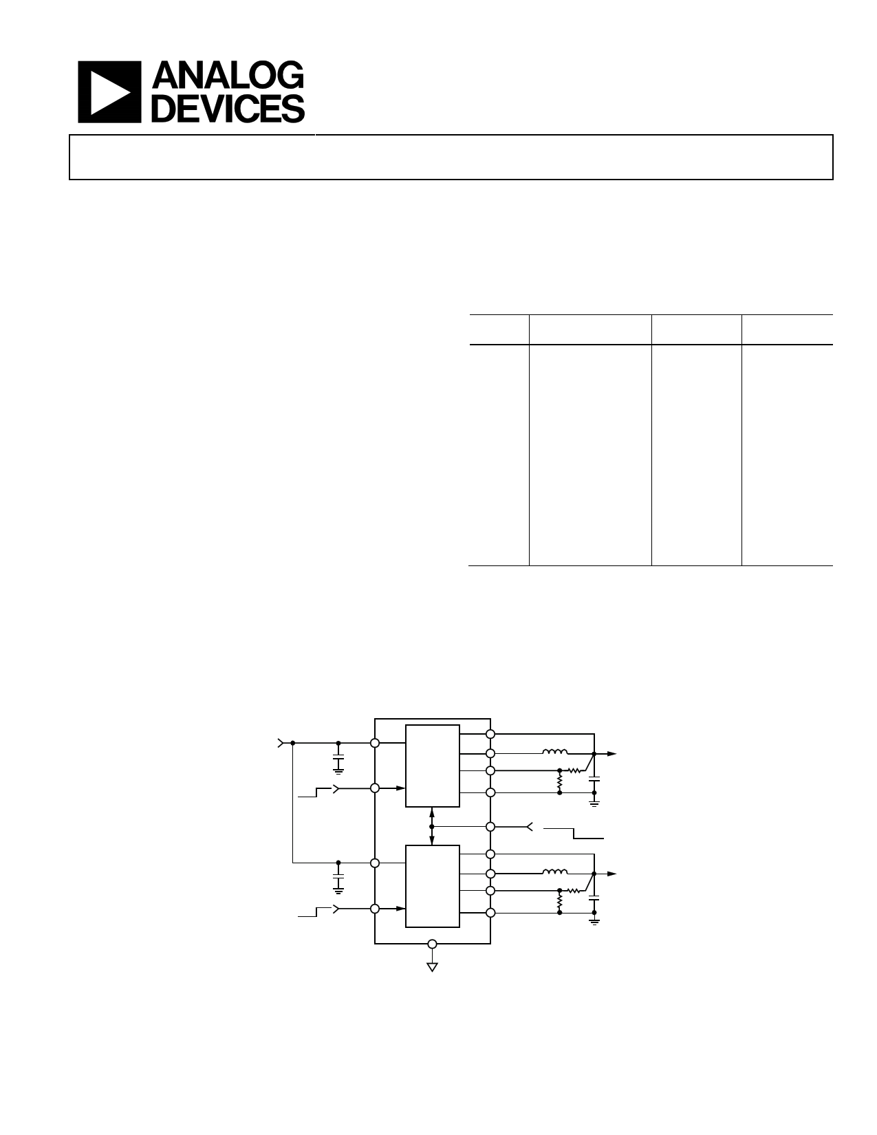
2.3V TO 5.5V
TYPICAL APPLICATION CIRCUIT
ADP5133
C1
4.7µF
VIN1
BUCK1
VOUT1
SW1
FB1
L1 1µH
R1
ON
OFF
EN1
PGND1
R2
VOUT1 @
800mA
C3
10µF
C2
4.7µF
ON
OFF
VIN2
EN2
BUCK2
MODE
FPWM
AUTO
VOUT2
SW2
L2 1µH
FB2 R3
PGND2
R4
VOUT2 @
800mA
C4
10µF
AGND
Figure 1.
Rev. 0
Document Feedback
Information furnished by Analog Devices is believed to be accurate and reliable. However, no
responsibilityisassumedbyAnalogDevices for itsuse,nor foranyinfringementsofpatentsor other
rights of third parties that may result from its use. Specifications subject to change without notice. No
license is granted by implication or otherwise under any patent or patent rights of Analog Devices.
Trademarksandregisteredtrademarksarethepropertyoftheirrespectiveowners.
One Technology Way, P.O. Box 9106, Norwood, MA 02062-9106, U.S.A.
Tel: 781.329.4700
©2014 Analog Devices, Inc. All rights reserved.
Technical Support
www.analog.com
1 page 
ADP5133
Data Sheet
BUCK1 AND BUCK2 SPECIFICATIONS
VIN1 = VIN2 = 2.3 V to 5.5 V; TJ = −40°C to +125°C for minimum/maximum specifications, and TA = 25°C for typical specifications, unless
otherwise noted. All limits at temperature extremes are guaranteed via correlation using standard statistical quality control (SQC).
Table 3.
Parameter
INPUT CHARACTERISTICS
Input Voltage Range
OUTPUT CHARACTERISTICS
Output Voltage Accuracy
Line Regulation
Load Regulation
VOLTAGE FEEDBACK
PSM CURRENT THRESHOLD
PSM to PWM Operation
OPERATING SUPPLY CURRENT
BUCK1 Only
BUCK2 Only
BUCK1 and BUCK2
Symbol
VIN1, VIN2
∆VOUT1/VOUT1, ∆VOUT2/VOUT2
(∆VOUT1/VOUT1)/∆VIN1,
(∆VOUT2/VOUT2)/∆VIN2
(∆VOUT1/VOUT1)/∆IOUT1,
(∆VOUT2/VOUT2)/∆IOUT2
VFB1, VFB2
IPSM
IIN
Test Conditions/Comments
PWM mode, ILOAD1 = ILOAD2 = 0 mA to 800 mA
PWM mode; ILOAD1 = ILOAD2 = 0 mA
PWM mode
ILOAD = 0 mA to 800 mA, PWM mode
MODE = ground
ILOAD1 = 0 mA, device not switching, all other
channels disabled
ILOAD2 = 0 mA, device not switching, all other
channels disabled
ILOAD1 = ILOAD2 = 0 mA, device not switching
Min Typ Max Unit
2.3 5.5 V
−1.8 +1.8 %
−0.05
%/V
−0.1 %/A
0.491 0.5 0.509 V
100 mA
44 µA
75 µA
87 µA
SWx CHARACTERISTICS
SWx On Resistance
Current Limit
ACTIVE PULL-DOWN
OSCILLATOR FREQUENCY
RPFET
RNFET
ILIMIT1, ILIMIT2
RPDWN-B
fSW
PFET at VIN1 = 5 V
PFET at VIN1 = 3.6 V
NFET at VIN1 = 5 V
NFET at VIN1 = 3.6 V
PFET switch peak current limit
VIN1 = VIN2 = 3.6 V, channels disabled
1100
2.5
145
180
110
125
1350
75
3.0
235
295
190
220
3.5
mΩ
mΩ
mΩ
mΩ
mA
Ω
MHz
INPUT AND OUTPUT CAPACITOR, RECOMMENDED SPECIFICATIONS
TA = −40°C to +125°C, unless otherwise specified.
Table 4.
Parameter
NOMINAL INPUT AND OUTPUT CAPACITOR RATINGS
BUCK1, BUCK2 Input Capacitor Rating
BUCK1, BUCK2 Output Capacitor Rating
CAPACITOR ESR
Symbol
CMIN1, CMIN2
CMIN1, CMIN2
CESR
Min
4.7
10
0.001
Typ Max Unit
40 µF
40 µF
1Ω
Rev. 0 | Page 4 of 24
5 Page 
ADP5133
T
VOUT
1
ISW
2
SW
4
CH1 50mV
CH2 500mA
CH4 2.00V
M 400ns A CH2
T 28.40%
220mA
Figure 21. Typical Waveforms, VOUT1 = 3.3 V, IOUT1 = 30 mA, PWM Mode
T
VOUT
1
ISW
2
SW
4
CH1 50mV
CH2 500mA
CH4 2.00V
M 400ns A CH2
T 28.40%
220mA
Figure 22. Typical Waveforms, VOUT2 = 1.8 V, IOUT2 = 30 mA, PWM Mode
T
VIN
VOUT
1
SW
3
CH1 50.0mV
CH3 1.00V
CH4 2.00V
M 1.00ms
T 30.40%
A CH3
4.80V
Figure 23. Buck1 Response to Line Transient, Input Voltage from 4.5 V to
5.0 V, VOUT1 = 3.3 V, PWM Mode
T
VIN
VOUT
1
SW
Data Sheet
43
CH1 50.0mV
CH3 1.00V
CH4 2.00V
M 1.00ms
T 30.40%
A CH3
4.80V
Figure 24. BUCK2 Response to Line Transient, VIN = 4.5 V to 5.0 V,
VOUT2 = 1.8 V, PWM Mode
T
SW
4
VOUT
1
IOUT
2
CH1 50.0mV
CH2 50.0mA
CH4 5.00V
M 20.0µs A CH2 356mA
T 60.000µs
Figure 25. BUCK1 Response to Load Transient, IOUT1 from 1 mA to 50 mA,
VOUT1 = 3.3 V, Auto PWM/PSM Mode
T
SW
4
VOUT
1
IOUT
2
CH1 50.0mV
CH2 50.0mA
CH4 5.00V
M 20.0µs A CH2
T 22.20%
379mA
Figure 26. BUCK2 Response to Load Transient, IOUT2 from 1 mA to 50 mA,
VOUT2 = 1.8 V, Auto PWM/PSM Mode
Rev. 0 | Page 10 of 24
11 Page | ||
| Páginas | Total 25 Páginas | |
| PDF Descargar | [ Datasheet ADP5133.PDF ] | |
Hoja de datos destacado
| Número de pieza | Descripción | Fabricantes |
| ADP5130 | Pressure sensor | Panasonic |
| ADP5131 | Pressure sensor | Panasonic |
| ADP5133 | 800 mA Buck Regulators | Analog Devices |
| ADP5134 | 1200 mA Buck Regulators and Two 300 mA LDO Regulators | Analog Devices |
| Número de pieza | Descripción | Fabricantes |
| SLA6805M | High Voltage 3 phase Motor Driver IC. |
Sanken |
| SDC1742 | 12- and 14-Bit Hybrid Synchro / Resolver-to-Digital Converters. |
Analog Devices |
|
DataSheet.es es una pagina web que funciona como un repositorio de manuales o hoja de datos de muchos de los productos más populares, |
| DataSheet.es | 2020 | Privacy Policy | Contacto | Buscar |