|
|
PDF SST25VF064C Data sheet ( Hoja de datos )
| Número de pieza | SST25VF064C | |
| Descripción | 64 Mbit SPI Serial Dual I/O Flash | |
| Fabricantes | SST | |
| Logotipo |  |
|
Hay una vista previa y un enlace de descarga de SST25VF064C (archivo pdf) en la parte inferior de esta página. Total 30 Páginas | ||
|
No Preview Available !
64 Mbit SPI Serial Dual I/O Flash
SST25VF064C
FEATURES:
SST25VF032B32Mb Serial Peripheral Interface (SPI) flash memory
Data Sheet
• Single Voltage Read and Write Operations
– 2.7-3.6V
• Serial Interface Architecture
– SPI Compatible: Mode 0 and Mode 3
• Dual Input/Output Support
– Fast-Read Dual-Output Instruction
– Fast-Read Dual I/O Instruction
• High Speed Clock Frequency
– 80 MHz for High-Speed Read (0BH)
– 75 MHz for Fast-Read Dual-Output (3BH)
– 50 MHz for Fast-Read Dual I/O (BBH)
– 33 MHz for Read Instruction (03H)
• Superior Reliability
– Endurance: 100,000 Cycles (typical)
– Greater than 100 years Data Retention
• Low Power Consumption
– Active Read Current: 12 mA (typical @ 80 MHz) for
single-bit read)
– Active Read Current: 14 mA (typical @ 75MHz) for
dual-bit read)
– Standby Current: 5 µA (typical)
• Flexible Erase Capability
– Uniform 4 KByte sectors
– Uniform 32 KByte overlay blocks
– Uniform 64 KByte overlay blocks
• Fast Erase
– Chip-Erase Time: 35 ms (typical)
– Sector-/Block-Erase Time: 18 ms (typical)
• Page-Program
– 256 Bytes per page
– Single and Dual Input support
– Fast Page-Program time in 1.5 ms (typical)
• End-of-Write Detection
– Software polling the BUSY bit in Status Register
• Write Protection (WP#)
– Enables/Disables the Lock-Down function of the
status register
• Software Write Protection
– Write protection through Block-Protection bits in sta-
tus register
• Security ID
– One-Time Programmable (OTP) 256 bit, Secure ID
- 64 bit Unique, Factory Pre-Programmed identifier
- 192 bit User-Programmable
• Temperature Range
– Commercial = 0°C to +70°C
– Industrial: -40°C to +85°C
• Packages Available
– 16-lead SOIC (300 mils)
– 8-contact WSON (6mm x 8mm)
– 8-lead SOIC (200 mils)
• All devices are RoHS compliant
PRODUCT DESCRIPTION
The SST 25 series Serial Flash family features a four-wire,
SPI-compatible interface that allows for a low pin-count
package which occupies less board space and ultimately
lowers total system costs. SST25VF064C SPI serial flash
memory is manufactured with SST proprietary, high-perfor-
mance CMOS SuperFlash technology. The split-gate cell
design and thick-oxide tunneling injector attain better reli-
ability and manufacturability compared with alternate
approaches.
The SST25VF064C significantly improves performance
and reliability, while lowering power consumption. The
device writes (Program or Erase) with a single power sup-
ply of 2.7-3.6V. The total energy consumed is a function of
the applied voltage, current, and time of application. Since
for any given voltage range, the SuperFlash technology
uses less current to program and has a shorter erase time,
the total energy consumed during any Erase or Program
operation is less than alternative flash memory technolo-
gies.
The SST25VF064C device is offered in 16-lead SOIC (300
mils), 8-contact WSON (6mm x 8mm), and 8-lead SOIC
(200 mils) packages. See Figure 2 for pin assignments.
©2010 Silicon Storage Technology, Inc.
S71392-04-000
04/10
1
The SST logo and SuperFlash are registered Trademarks of Silicon Storage Technology, Inc.
These specifications are subject to change without notice.
1 page 
64 Mbit SPI Serial Dual I/O Flash
SST25VF064C
Reset/Hold Mode
The RST#/HOLD# pin provides either a hardware reset or
a hold pin. From power-on, the RST#/HOLD# pin defaults
as a hardware reset pin (RST#). The Hold mode for this pin
is a user selected option where an EHLD instruction
enables the Hold mode. Once selected as a hold pin
(HOLD#), the RST#/HOLD# pin will be configured as a
HOLD# pin, and goes back to RST# pin only after a power-
off and power-on sequence.
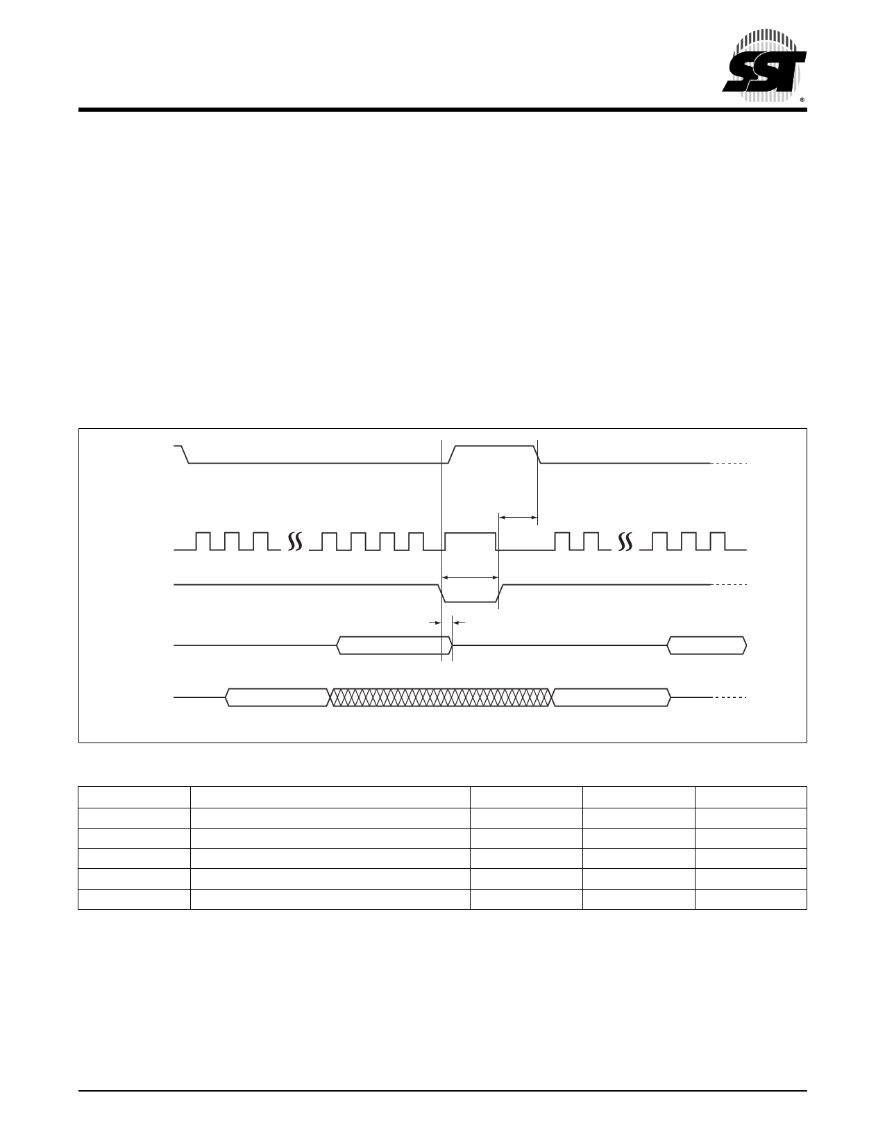
Reset
If the RST#/HOLD# pin is used as a reset pin, RST# pin
provides a hardware method for resetting the device. Driving
the RST# pin high puts the device in normal operating
Data Sheet
mode. The RST# pin must be driven low for a minimum of
TRST time to reset the device. The SO pin is in high imped-
ance state while the device is in reset. A successful reset will
reset the status register to its power-up state (BPL, BUSY
and WEL = 0; BP3, BP2, BP1, and BP0 = 1). See Table 2
for default power-up modes. A device reset during an active
Program or Erase operation aborts the operation and data
of the targeted address range may be corrupted or lost due
to the aborted erase or program operation.
CE#
SCK
RST#
SO
SI
FIGURE 4: Reset Timing Diagram
TABLE 2: Reset Timing Parameters
Symbol
TRST
TRHZ
TRECR
TRECP
TRECE
Parameter
Reset Pulse Width
Reset to High-Z Output
Reset Recovery from Read
Reset Recovery from Program
Reset Recovery from Erase
TRECR
TRECP
TRECE
TRST
TRHZ
Min
100
1292 F28.0
Max
105
100
10
1
Units
ns
ns
ns
µs
ms
T2.1392
©2010 Silicon Storage Technology, Inc.
5
S71392-04-000
04/10
5 Page 
64 Mbit SPI Serial Dual I/O Flash
SST25VF064C
Data Sheet
CE#
MODE 3
SCK MODE 0
012 345 6 78
15 16 23 24 31 32 39 40 47 48 55 56 63 64 71 72 80
SI 0B ADD. ADD. ADD.
SO HIGH IMPEDANCE
FIGURE 7: High-Speed Read Sequence
X
N
DOUT
MSB
N+1
DOUT
N+2 N+3 N+4
DOUT DOUT DOUT
1392 F07.0
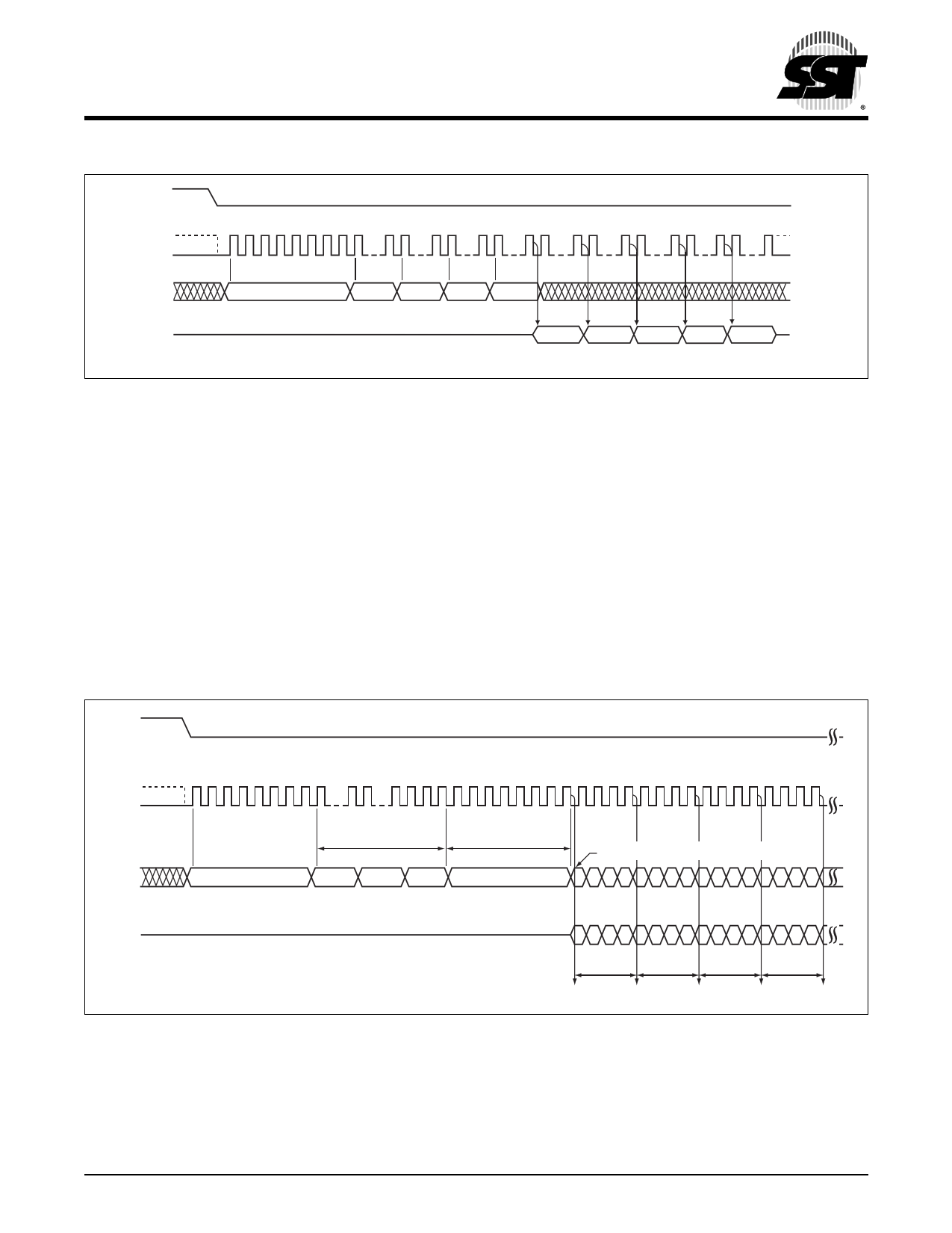
Fast-Read Dual-Output (75 MHz)
The Fast-Read Dual-Output (3BH) instruction outputs data
up to 75 MHz from the SIO0 and SIO1 pins. To initiate the
instruction, execute an 8-bit command (3BH) followed by
address bits A23-A0 and a dummy byte on SI/SIO0. Fol-
lowing a dummy cycle, the Fast-Read Dual-Output instruc-
tion outputs the data starting from the specified address
location on the SIO1 and SIO0 lines. SIO1 outputs, per
clock sequence, odd data bits D7, D5, D3, and D1; and
SIO0 outputs even data bits D6, D4, D2, and D0. CE# must
remain active low for the duration of the Fast-Read Dual-
Output instruction cycle. See Figure 8 for the Fast-Read
Dual-Output sequence.
The data output stream is continuous through all
addresses until terminated by a low-to-high transition on
CE#. The internal address pointer will automatically incre-
ment until the highest memory address is reached. Once
the highest memory address is reached, the address
pointer automatically increments to the beginning (wrap-
around) of the address space. for 64 Mbit density, once the
data from address location 7FFFFFH has been read the
next output will be from address location 000000H.
CE#
SCK
MODE 3
MODE 0
0 1 23 456 78
15 16 28 29 30 31 32 33 34 35 36 37 38 39 40 41 42 43 44 45 46 47 48 49 50 51 52 53 54 55
SIO0
SIO1
24-Bit Address
3B ADD. ADD. ADD.
HIGH IMPEDANCE
FIGURE 8: Fast-Read Dual Output Sequence
Dummy Cycle
X
IO, Switches from Input to Output
642 0642 0642 0642 0
DOUT DOUT DOUT DOUT
75 3 1 75 31 75 31 75 31
MSB MSB MSB MSB
N N+1 N+2 N+3
1392 F08.1
©2010 Silicon Storage Technology, Inc.
11
S71392-04-000
04/10
11 Page | ||
| Páginas | Total 30 Páginas | |
| PDF Descargar | [ Datasheet SST25VF064C.PDF ] | |
Hoja de datos destacado
| Número de pieza | Descripción | Fabricantes |
| SST25VF064C | 64 Mbit SPI Serial Dual I/O Flash | Microchip |
| SST25VF064C | 64 Mbit SPI Serial Dual I/O Flash | SST |
| Número de pieza | Descripción | Fabricantes |
| SLA6805M | High Voltage 3 phase Motor Driver IC. |
Sanken |
| SDC1742 | 12- and 14-Bit Hybrid Synchro / Resolver-to-Digital Converters. |
Analog Devices |
|
DataSheet.es es una pagina web que funciona como un repositorio de manuales o hoja de datos de muchos de los productos más populares, |
| DataSheet.es | 2020 | Privacy Policy | Contacto | Buscar |
