|
|
|
PDF SIC645 Data sheet ( Hoja de datos )
| Número de pieza | SIC645 | |
| Descripción | 60A VRPower Smart Power Stage (SPS) Module | |
| Fabricantes | Vishay | |
| Logotipo | ||
Hay una vista previa y un enlace de descarga de SIC645 (archivo pdf) en la parte inferior de esta página. Total 18 Páginas | ||
|
No Preview Available !
www.vishay.com
SiC645
Vishay Siliconix
60 A VRPower® Smart Power Stage (SPS) Module with Integrated
High-Accuracy Current and Temperature Monitors
DESCRIPTION
The SiC645 is a smart VRPower® device that integrates a
high side and low side MOSFET, a high performance driver
with integrated bootstrap FET. The SiC645 offers high
accuracy current and temperature monitors that can be fed
back to the controller and doubler to complete a multiphase
DC/DC system. They simplify design and increase
performance by eliminating the DCR sensing network and
associated thermal compensation. Light-load efficiency is
supported via a dedicated left control pin. An industry
leading thermally enhanced dual cooled, 5 mm x 5 mm
PowerPAK® MLP package allows minimal overall PCB real
estate and low-profile construction.
The devices feature a 3.3 V (SiC645A) or 5 V (SiC645)
compatible tri-state PWM input that, working together with
multiphase PWM controllers, will provide a robustsolution in
the event of abnormal operating conditions. The SiC645
also improves system performance and reliability with
integrated fault protection of UVLO, over-temperature and
over-current. An open-drain fault reporting pin simplifies the
handshake between the smart VRPower device and
multiphase controllers and can be used to disable the
controller during start-up and fault conditions.
FEATURES
• Input range: 4.5 V to 18 V
• Supports 60 A DC current
• Compatible with 3.3 V (SiC645A) and 5 V
(SiC645) tri-state PWM
• Down slope current sensing
• ± 3 % accuracy current monitor (IMON) with REFIN input
• 8 mV/°C temperature monitor with OT flag
• Dedicated low-side FET control input
• Fault protection
- High-side FET short and over-current protection
- Over-temperature protection
- VCC and VIN under voltage lockout (UVLO)
• Open drain fault reporting output
• Up to 2 MHz switching frequency
• Material categorization: for definitions of compliance
please see www.vishay.com/doc?99912
APPLICATIONS
• High frequency and high efficiency VRM and VRD
• Core, graphic, and memory regulators for microprocessors
• High density VR for server, networking, and cloud computing
• POL DC/DC converters and video gaming consoles
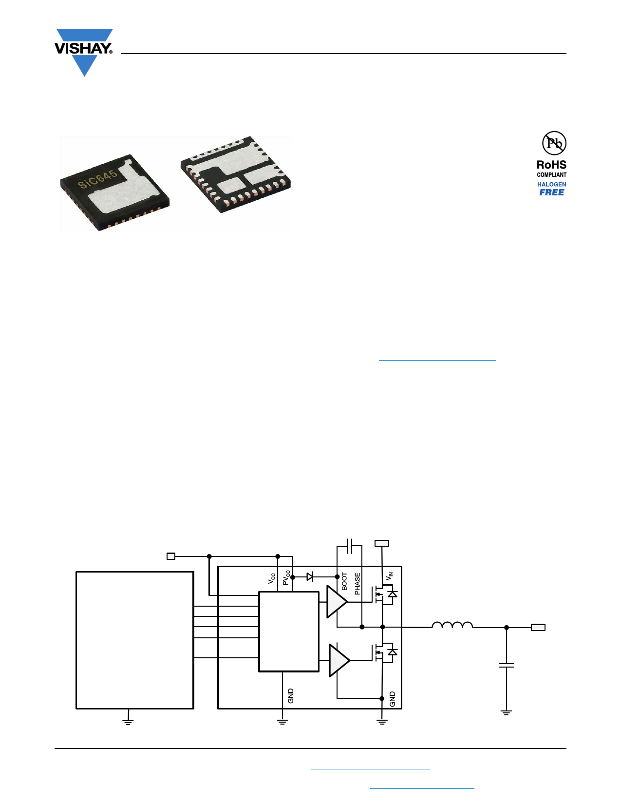
TYPICAL APPLICATION DIAGRAM
+5 V
+12 V
VCC
Multiphase
controller
PWM
CS#n
CSRTN#n
TEMP
EN
LGCTRL
PWM
IMON
REFIN
TMON
FAULT#
Shoot-
through
protection
Smart
control
PVCC
SW
LOUT
VOUT
COUT
GND
SiC645
Fig. 1 - SiC645 Typical Application Block Diagram
S16-2233-Rev. B, 31-Oct-16
1
Document Number: 65424
For technical questions, contact: [email protected]
THIS DOCUMENT IS SUBJECT TO CHANGE WITHOUT NOTICE. THE PRODUCTS DESCRIBED HEREIN AND THIS DOCUMENT
ARE SUBJECT TO SPECIFIC DISCLAIMERS, SET FORTH AT www.vishay.com/doc?91000
1 page 
www.vishay.com
PINOUT CONFIGURATION
SiC645
Vishay Siliconix
32 31 30 29 28 27 26 25 24
LGCTRL 1
VCC 2
PVCC 3
GND 4
GND
33
23 VIN
VIN 22 VIN
34 21 VIN
GL 5
20 GND
GND 6
GND 7
GND 8
GND
35
19 GND
18 GND
17 GND
9 10 11 12 13 14 15 16
Fig. 5 - SiC645 Pinout Configuration
PIN CONFIGURATION
PIN NUMBER
NAME
1 LGCTRL
2
3
4, 6, 7, 8, 17, 18,
19, 20, 29, 33, 35
5
9, 10, 11, 12,
13, 14, 15, 16
21, 22, 23, 27,
34
24
25
VCC
PVCC
GND
NC
SW
VIN
PHASE
BOOT
26 FAULT#
28 PWM
30 REFIN
31 IMON
32 TMON
FUNCTION
Lower gate control signal input. LO = GL LO (LFET off). HI = normal operation (GL and GH strictly obey
PWM). This pin should be driven with a logic signal, or externally tied high if not required; it should not
be left floating.
+5 V logic bias supply. Place a high quality low ESR ceramic capacitor (~1 μF/X7R) in close proximity
from this pin to GND.
+5 V gate drive bias supply. Place a high quality low ESR ceramic capacitor (~1 μF/X7R) in close
proximity from this pin to GND.
GND pins are internally connected. Pins 4 and 29 should be connected directly to the nearby GND
paddles on package bottom. Fig. 15 shows GND paddles should be connected to the system GND
plane with as many vias as possible to maximize thermal and electrical performance.
No connect (This is a low-side gate driver output (GL), optional to monitor for system debugging).
Switching junction node between HFET source and LFET drain. Connect directly to output inductor.
Input of power stage (to drain of HFET). Place at least 2 ceramic capacitors (10 μF or higher, X5R or
X7R) in close proximity across VIN and GND. Pin 27 should not be used for decoupling. For optimal
performance, place as many vias as possible in the bottom side VIN paddle.
Return of boot capacitor. Internally connected to SW node so no external routing required for SW
connection.
Floating bootstrap supply pin for the upper gate drive. Place a high quality low ESR ceramic capacitor
(0.1 μF/X7R to 0.22 μF/X7R)i n close proximity across BOOT and PHASE pins.
Open drain output pin. Any fault (over-current, over-temperature, shorted HFET, or POR / UVLO) will
pull this pin to ground. This pin may be connected to the controller enable pin or used to signal a fault
at the system level.
PWM input of gate driver, compatible with 3.3 V and 5 V tri-state PWM signal.
Input for external reference voltage for IMON signal. This voltage should be between 0.8 V and 1.6 V.
Connect REFIN to the appropriate current sense input of the controller. Place a high quality low ESR
ceramic capacitor (~ 0.1 μF) in close proximity from this pin to GND.
Current monitor output, referenced to REFIN. IMON will be pulled high (to REFIN +1.2 V) to indicate an
HFET shorted or over-current fault. Connect the IMON output to the appropriate current sense input of
the controller. No more than 56 pF capacitance can be directly connected across IMON and REFIN pins.
With a 100 series resistor, up to 470 pF may be used.
Temperature monitor output. For multiphase, the TMON pins can be connected together as a common
bus; the highest voltage (representing the highest temperature) will be sent to the PWM controller.
TMON will be pulled high (to 2.5 V) to indicate an over-temperature fault. No more than 250 pF total
capacitance can be directly connected across TMON and GND pins; with a series resistor, a higher
capacitance load is allowed, such as 1 k for 100 nF load.
S16-2233-Rev. B, 31-Oct-16
5
Document Number: 65424
For technical questions, contact: [email protected]
THIS DOCUMENT IS SUBJECT TO CHANGE WITHOUT NOTICE. THE PRODUCTS DESCRIBED HEREIN AND THIS DOCUMENT
ARE SUBJECT TO SPECIFIC DISCLAIMERS, SET FORTH AT www.vishay.com/doc?91000
5 Page 
www.vishay.com
SiC645
Vishay Siliconix
The HFET current is not monitored in the same way, so no
valid measured current is available while PWM is high (and
the short delays before and after). During this time, the
IMON will output the last valid LFET current before the
sampling stopped. On start-up after POR, the IMON will
output zero (relative to REFIN, which represents zero current)
until the switching begins, and then the current can be
properly measured.
The high-side FET current is separately monitored for OC
conditions; see the “over-current protection” section.
Over-current Protection
Fig. 14 shows the timing diagram of an over-current fault.
There is a comparator monitoring the HFET current while it
is on (GH high; also requires VIN POR above its trip point).
If the current is higher than 90 A (typical; not
user-programmable), then an OC fault is detected. The GH
will be forced low, even if PWM is still high; this effectively
shortens the PWM (and GH) pulse width, to limit the current.
The IMON pin is pulled up to REFIN +1.2 V, which will be
detected by the controller as an over-current fault. The
controller is then expected to force PWM to tri-state (which
gates off both FETs) or low state (turns on LFET), either of
which signals the SPS that the fault has been
acknowledged. This starts a ~ 1 μs fault clear delay. The
IMON flag is released after the delay. The driver will then
respond to PWM inputs normally.
Note that if the controller does NOT acknowledge, the IMON
flag will stay high indefinitely, which will also hold GH low.
If OC is detected, the FAULT# pin is also pulled low; the
timing on the FAULT# pin will follow that of the IMON pin.
ILIM
HFET
current
0
GH
GL
PWM
1.2 V
IMON-REFIN
No GH allowed
FollowPWM low to
support OV following OC
DMP enters PWM mid-state
or low to acknowledge fault
Fault#
Fault
clear
delay
1 μs
Resume
normal O P
(if recovers)
Fig. 14 - Over-current Fault Timing Diagram
Shorted HFET Protection
In the case of a shorted HFET, the SW node will have
excessive positive voltage present even when the LFET is
turned on. The SiC645 monitors the SW node during periods
when the LFET is on (GL is high), and should that voltage
exceed 100 mV (typical), the HFET short fault is declared.
The SiC645 will pull the IMON pin high, and the FAULT# will
be pulled low. But the fault will be latched; VCC POR is
needed to reset it. GH will be gated low (ignore PWM = high),
but the SiC645 will still respond to PWM tri-state and logic
low.
Thermal Monitoring
The SiC645 monitors its internal temperature and provides
a signal proportional to that temperature on the TMON pin.
TMON has a voltage of 600 mV at 0 °C and reflects
temperature at 8 mV/°C. The TMON output is valid 125 μs
after VCC POR.
600 mV + 8 mV/°C x temperature
Over-temperature
Fault
reporting
configuration
TMON pin
Fig. 15 - Over-Temperature Fault
Fig. 15 shows a simplified functional representation. The top
section includes the sensor and the output buffer. The
bottom section includes the protection sensing, that will pull
the output high. The TMON pin is configured internally such
that a user can tie multiple pins together externally and the
resulting TMON bus will assume the voltage of the highest
contributor (representing the highest temperature).
Thermal Protection
If the internal temperature exceeds the over-temperature
trip point (+140 °C typical), the TMON pin is pulled high (to
~2.5 V), and the FAULT# pin is pulled low. No other action is
taken on-chip. Both the TMON and FAULT# pins will remain
in the fault mode, until the junction temperature drops below
+125 °C typical; at that point, the TMON and FAULT# pins
resume normal operation; the DMP can detect that the fault
condition has gone away, and decide what to do next.
FAULT Reporting
Over-current and shorted HFET detections will pull the
IMON pin to a high (fault) level, such that the DMP should
quickly recognize it as out of the normal range.
Over-temperature detection will pull the TMON pin to a high
(fault) level, such that the PWM controller should quickly
recognize it as out of the normal range.
All of the above faults, plus the VCC and VIN POR (UVLO)
conditions, will also pull down the FAULT# pin. This can be
used by the controller (or system) as fault detection, and can
also be used to disable the controller, through its enable pin.
The fault reporting and respective SPS response are
summarized in Table 2.
S16-2233-Rev. B, 31-Oct-16
11
Document Number: 65424
For technical questions, contact: [email protected]
THIS DOCUMENT IS SUBJECT TO CHANGE WITHOUT NOTICE. THE PRODUCTS DESCRIBED HEREIN AND THIS DOCUMENT
ARE SUBJECT TO SPECIFIC DISCLAIMERS, SET FORTH AT www.vishay.com/doc?91000
11 Page | ||
| Páginas | Total 18 Páginas | |
| PDF Descargar | [ Datasheet SIC645.PDF ] | |
Hoja de datos destacado
| Número de pieza | Descripción | Fabricantes |
| SIC645 | 60A VRPower Smart Power Stage (SPS) Module | Vishay |
| Número de pieza | Descripción | Fabricantes |
| SLA6805M | High Voltage 3 phase Motor Driver IC. |
Sanken |
| SDC1742 | 12- and 14-Bit Hybrid Synchro / Resolver-to-Digital Converters. |
Analog Devices |
|
DataSheet.es es una pagina web que funciona como un repositorio de manuales o hoja de datos de muchos de los productos más populares, |
| DataSheet.es | 2020 | Privacy Policy | Contacto | Buscar |