|
|
|
PDF M24C08-125 Data sheet ( Hoja de datos )
| Número de pieza | M24C08-125 | |
| Descripción | serial I2C bus EEPROM | |
| Fabricantes | STMicroelectronics | |
| Logotipo | ||
Hay una vista previa y un enlace de descarga de M24C08-125 (archivo pdf) en la parte inferior de esta página. Total 30 Páginas | ||
|
No Preview Available !
M24C16-125 M24C08-125
M24C04-125 M24C02-125
Automotive 16-Kbit, 8-Kbit, 4-Kbit and 2-Kbit
serial I²C bus EEPROM
Datasheet − production data
Features
■ Compatible with I²C bus modes:
– 400 kHz Fast mode
)– 100 kHz Standard mode
t(s■ Memory array:
c– 2 Kb, 4 Kb, 8 Kb, 16 Kb of EEPROM
u– Page size: 16 bytes
rod■ Write
P– Byte Write within 5 ms
te– Page Write within 5 ms
le■ Single supply voltage:
o– 2.5 V to 5.5 V
bs■ Operating temperature range: -40°C up to
+125°C
- O■ Random and sequential Read modes
t(s)■ Automatic address incrementing
■ Write protect of the whole memory array
uc■ Enhanced ESD/Latch-Up protection
rod■ More than 1 million Write cycles
P■ More than 40-year data retention
te■ Packages
le– RoHS-compliant and halogen-free
Obso(ECOPACK2®)
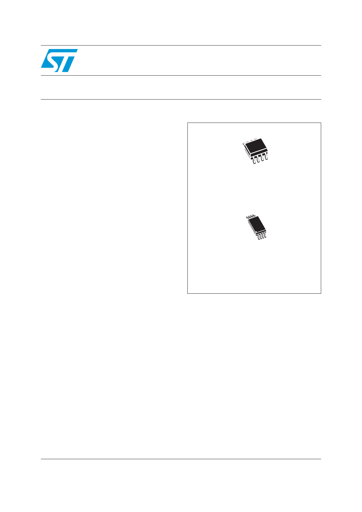
SO8 (MN)
150 mils width
TSSOP8 (DW)
169 mils width
March 2012
This is information on a product in full production.
Doc ID 022564 Rev 1
1/30
www.st.com
1
1 page 
M24C16-125 M24C08-125 M24C04-125 M24C02-125
List of figures
List of figures
Figure 1. Logic diagram . . . . . . . . . . . . . . . . . . . . . . . . . . . . . . . . . . . . . . . . . . . . . . . . . . . . . . . . . . . . 6
Figure 2. 8-pin package connections (top view) . . . . . . . . . . . . . . . . . . . . . . . . . . . . . . . . . . . . . . . . . 6
Figure 3.
Figure 4.
Figure 5.
Device select code . . . . . . . . . . . . . . . . . . . . . . . . . . . . . . . . . . . . . . . . . . . . . . . . . . . . . . . . 7
I2C Fast mode (fC = 400 kHz): maximum Rbus value versus bus parasitic
capacitance (Cbus) . . . . . . . . . . . . . . . . . . . . . . . . . . . . . . . . . . . . . . . . . . . . . . . . . . . . . . . . 9
I²C bus protocol . . . . . . . . . . . . . . . . . . . . . . . . . . . . . . . . . . . . . . . . . . . . . . . . . . . . . . . . . . 9
Figure 6. Write mode sequences with WC = 1 (data write inhibited) . . . . . . . . . . . . . . . . . . . . . . . . . 13
Figure 7. Write mode sequences with WC = 0 (data write enabled) . . . . . . . . . . . . . . . . . . . . . . . . . 15
Figure 8.
)Figure 9.
t(sFigure 10.
Figure 11.
ucFigure 12.
Obsolete Product(s) - Obsolete ProdFigure 13.
Write cycle polling flowchart using ACK . . . . . . . . . . . . . . . . . . . . . . . . . . . . . . . . . . . . . . . 16
Read mode sequences . . . . . . . . . . . . . . . . . . . . . . . . . . . . . . . . . . . . . . . . . . . . . . . . . . . . 17
AC measurement I/O waveform . . . . . . . . . . . . . . . . . . . . . . . . . . . . . . . . . . . . . . . . . . . . . 20
AC waveforms . . . . . . . . . . . . . . . . . . . . . . . . . . . . . . . . . . . . . . . . . . . . . . . . . . . . . . . . . . 24
SO8 narrow – 8 lead plastic small outline, 150 mils body width, package outline . . . . . . . 26
TSSOP8 – 8 lead thin shrink small outline, package outline . . . . . . . . . . . . . . . . . . . . . . . 27
Doc ID 022564 Rev 1
5/30
5 Page 
M24C16-125 M24C08-125 M24C04-125 M24C02-125
3 Device operation
Device operation
The device supports the I²C protocol. This is summarized in Figure 5. Any device that sends
data on to the bus is defined to be a transmitter, and any device that reads the data to be a
receiver. The device that controls the data transfer is known as the bus master, and the
other as the slave device. A data transfer can only be initiated by the bus master, which will
also provide the serial clock for synchronization. The device is always a slave in all
communication.
3.1 Start condition
t(s)Start is identified by a falling edge of Serial Data (SDA) while Serial Clock (SCL) is stable in
the High state. A Start condition must precede any data transfer command. The device
ccontinuously monitors (except during a Write cycle) Serial Data (SDA) and Serial Clock
u(SCL) for a Start condition.
Prod3.2 Stop condition
leteStop is identified by a rising edge of Serial Data (SDA) while Serial Clock (SCL) is stable
oand driven High. A Stop condition terminates communication between the device and the
sbus master. A Read command that is followed by NoAck can be followed by a Stop condition
bto force the device into the Standby mode. A Stop condition at the end of a Write command
Otriggers the internal Write cycle.
t(s) -3.3 Acknowledge bit (ACK)
ucThe acknowledge bit is used to indicate a successful byte transfer. The bus transmitter,
dwhether it be bus master or slave device, releases Serial Data (SDA) after sending eight bits
roof data. During the 9th clock pulse period, the receiver pulls Serial Data (SDA) Low to
Packnowledge the receipt of the eight data bits.
olete3.4 Data input
bs During data input, the device samples Serial Data (SDA) on the rising edge of Serial Clock
O (SCL). For correct device operation, Serial Data (SDA) must be stable during the rising edge
of Serial Clock (SCL), and the Serial Data (SDA) signal must change only when Serial Clock
(SCL) is driven Low.
Doc ID 022564 Rev 1
11/30
11 Page | ||
| Páginas | Total 30 Páginas | |
| PDF Descargar | [ Datasheet M24C08-125.PDF ] | |
Hoja de datos destacado
| Número de pieza | Descripción | Fabricantes |
| M24C08-125 | serial I2C bus EEPROM | STMicroelectronics |
| Número de pieza | Descripción | Fabricantes |
| SLA6805M | High Voltage 3 phase Motor Driver IC. |
Sanken |
| SDC1742 | 12- and 14-Bit Hybrid Synchro / Resolver-to-Digital Converters. |
Analog Devices |
|
DataSheet.es es una pagina web que funciona como un repositorio de manuales o hoja de datos de muchos de los productos más populares, |
| DataSheet.es | 2020 | Privacy Policy | Contacto | Buscar |