|
|
PDF MCP1711 Data sheet ( Hoja de datos )
| Número de pieza | MCP1711 | |
| Descripción | Capacitorless LDO Regulator | |
| Fabricantes | Microchip | |
| Logotipo |  |
|
Hay una vista previa y un enlace de descarga de MCP1711 (archivo pdf) en la parte inferior de esta página. Total 30 Páginas | ||
|
No Preview Available !
MCP1711
150 mA Ultra-Low Quiescent Current, Capacitorless LDO Regulator
Features
• Low Quiescent Current: 600 nA
• Input Voltage Range: 1.4V to 6.0V
• Standard Output Voltages: 1.2V, 1.8V, 1.9V, 2.2V,
2.5V, 3.0V, 3.3V, 5.0V
• Output Accuracy: ±20 mV for 1.2V and 1.8V
options and ±1% for VR > 2.0V
• Temperature Stability: ±50 ppm/°C
• Maximum Output Current: 150 mA;
• Low ON Resistance: 3.3 @ VR = 3.0V
• Standby Current: 10 nA
• Protection Circuits: Current Limiter, Short Circuit,
Foldback
• SHDN Pin Function: ON/OFF Logic = Enable
High
• COUT Discharge Circuit when SHDN Function is
Active
• Output Capacitor: Low Equivalent Series
Resistance (ESR) Ceramic, Capacitorless
Compatible
• Operating Temperature: -40°C – +85°C
(Industrial)
• Available Packages:
- 4-Lead 1 x 1 mm UQFN
- 5-Lead SOT-23
• Environmentally Friendly: EU RoHS Compliant,
Lead-Free
Applications
• Energy Harvesting
• Long-Life, Battery-Powered Applications
• Portable Electronics
• Ultra-Low Consumption “Green” Products
• Mobile Devices/Terminals
• Wireless LAN
• Modules (Wireless, Cameras)
Related Literature
• AN765, Using Microchip’s Micropower LDOs
(DS00765), Microchip Technology Inc.
• AN766, Pin-Compatible CMOS Upgrades to
Bipolar LDOs (DS00766),
Microchip Technology Inc.
• AN792, A Method to Determine How Much Power
a SOT23 Can Dissipate in an Application
(DS00792), Microchip Technology Inc.
General Description
The MCP1711 is a highly accurate CMOS low dropout
(LDO) voltage regulator that can deliver up to 150 mA
of current while consuming only 0.6 µA of quiescent
current (typical). The input operating range is specified
from 1.4V to 6.0V, making it an ideal choice for mobile
applications and one-cell Li-Ion powered applications.
The MCP1711 is capable of delivering 150 mA output
current with only 0.32V (typical) for VR = 5.0V, and
1.41V (typical) for VR = 1.2V of input-to-output voltages
differential. The output voltage accuracy of the
MCP1711 is typically ± 0.02V for VR < 2.0V and ±1% for
VR > 2.0V at +25°C. The temperature stability is
approximately ±50 ppm/°C. Line regulation is
±0.01%/V typical at +25°C.
The output voltages available for the MCP1711 range
from 1.2V to 5.0V. The LDO output is stable even if an
output capacitor is not connected, due to an excellent
internal phase compensation. However, for better tran-
sient responses, the output capacitor should be added.
The MCP1711 is compatible with low ESR ceramic
output capacitors.
Overcurrent limit and short-circuit protection embed-
ded into the device provide a robust solution for any
application.
The MCP1711 has a true current foldback feature.
When the load decreases beyond the MCP1711 load
rating, the output current and output voltage will fold-
back toward 80 mA (typical) at approximately 0V out-
put. When the load impedance increases and returns to
the rated load, the MCP1711 will follow the same fold-
back curve as the device comes out of current
foldback.
If the device is in Shutdown mode, by inputting a
low-level signal to the SHDN pin, the current consump-
tion is reduced to less than 0.1 µA (typically 0.01 µA).
In Shutdown mode, if the output capacitor is used, it will
be discharged via the internal dedicated switch and, as
a result, the output voltage quickly returns to 0V.
The package options for the MCP1711 are the 4-lead
1 x 1 mm UQFN and the 5-lead SOT-23, which makes
the device ideal for small and compact applications.
2015 Microchip Technology Inc.
DS20005415B-page 1
1 page 
MCP1711
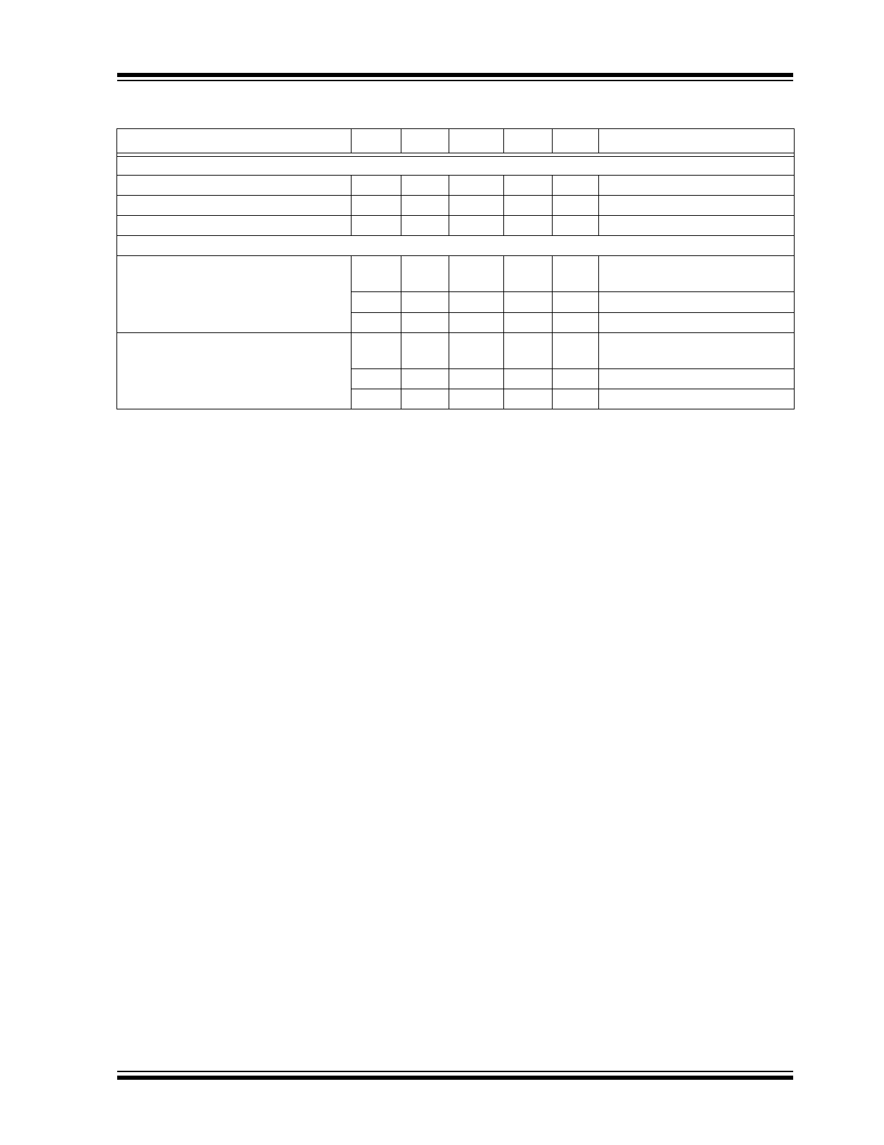
TEMPERATURE SPECIFICATIONS (1)
Parameters
Sym. Min. Typ. Max. Units
Conditions
Temperature Ranges
Operating Ambient Temperature Range
Junction Operating Temperature
Storage Temperature Range
Package Thermal Resistances
TA
TJ
TA
-40
-40
-55
— +85 °C
— +125 °C
— +125 °C
Thermal Resistance, 1 x 1 UQFN-4Ld JA
— 181.82 — °C/W JEDEC 51-7 FR4 board with
thermal vias
JA — 1000 — °C/W (2)
JC — 15 — °C/W
Thermal Resistance, SOT-23-5Ld
JA — 166.67 — °C/W JEDEC 51-7 FR4 board with
thermal vias
JA — 400 — °C/W (2)
JC — 81 — °C/W
Note 1: The maximum allowable power dissipation is a function of ambient temperature, the maximum allowable
junction temperature, and the thermal resistance from junction to air (i.e., TA, TJ, JA). Exceeding the max-
imum allowable power dissipation will cause the device operating junction temperature to exceed the
maximum +125°C rating. Sustained junction temperatures above +125°C can impact the device reliability.
2: The device is mounted on one layer PCB with minimal copper that does not provide any additional cooling.
2015 Microchip Technology Inc.
DS20005415B-page 5
5 Page 
MCP1711
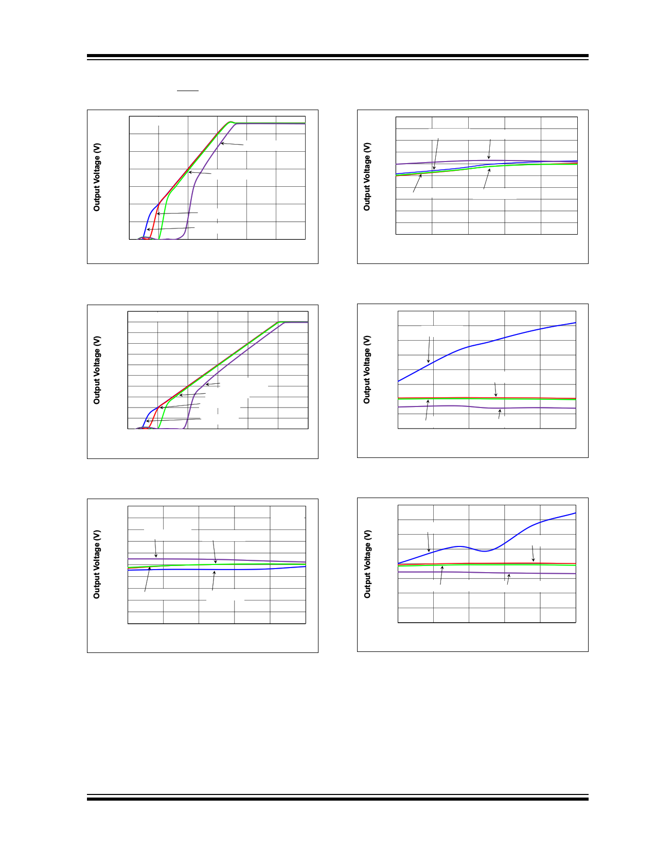
Note: Unless otherwise indicated, VIN = 3.5V for VR < 2.5V or VIN = VR + 1V for VR 2.5V, IOUT = 1 mA,
CIN = COUT = 0 µF, VSHDN = VIN, TA = +25°C.
3.50
3.00
VR = 3.3V
2.50
2.00
1.50
1.00
0.50
0.00
0
1
FIGURE 2-31:
Voltage.
IOUT = 100 mA
IOUT = 10 mA
IOUT = 1 mA
IOUT = 1 µA
23456
Input Voltage (V)
Output Voltage vs. Input
1.85
1.84
1.83
IOUT = 1 µA
IOUT = 100 mA
VR = 1.8V
1.82
1.81
1.80
1.79
1.78
IOUT = 1 mA
IOUT = 10 mA
1.77
1.76
1.75
-40 -15 10 35 60 85
Ambient Temperature (°C)
FIGURE 2-34:
Temperature.
Output Voltage vs. Ambient
5.50
5.00 VVRR==55..00VV
4.50
4.00
3.50
3.00
2.50
2.00
1.50
1.00
0.50
0.00
0
1
FIGURE 2-32:
Voltage.
IOUT = 100 mA
IOUT = 10 mA
IOUT = 1 mA
IOUT = 1 µA
23456
Input Voltage (V)
Output Voltage vs. Input
3.60
3.55
3.50
VR = 3.3V
IOUT = 1 µA
3.45
3.40
3.35
IOUT = 1 mA
3.30
3.25
3.20
-40
IOUT = 10 mA
IOUT = 100 mA
-15 10 35 60
Ambient Temperature (°C)
85
FIGURE 2-35:
Temperature.
Output Voltage vs. Ambient
1.25
1.24
1.23
1.22
IOUT = 100 mA
IOUT = 10 mA
1.21
1.20
1.19
1.18
1.17
IOUT = 1 mA
IOUT = 1 µA
1.16
1.15
-40 -15 10 35
VR = 1.2V
60 85
Ambient Temperature (°C)
FIGURE 2-33:
Temperature.
Output Voltage vs. Ambient
5.20
5.15
5.10
5.05
VR = 5.0V
IOUT = 1 µA
IOUT = 1 mA
5.00
4.95
4.90
IOUT = 10 mA
IOUT = 100 mA
4.85
4.80
-40 -15 10 35 60 85
Ambient Temperature (°C)
FIGURE 2-36:
Temperature.
Output Voltage vs. Ambient
2015 Microchip Technology Inc.
DS20005415B-page 11
11 Page | ||
| Páginas | Total 30 Páginas | |
| PDF Descargar | [ Datasheet MCP1711.PDF ] | |
Hoja de datos destacado
| Número de pieza | Descripción | Fabricantes |
| MCP1710 | Ultra Low Quiescent Current LDO Regulator | Microchip |
| MCP1711 | Capacitorless LDO Regulator | Microchip |
| Número de pieza | Descripción | Fabricantes |
| SLA6805M | High Voltage 3 phase Motor Driver IC. |
Sanken |
| SDC1742 | 12- and 14-Bit Hybrid Synchro / Resolver-to-Digital Converters. |
Analog Devices |
|
DataSheet.es es una pagina web que funciona como un repositorio de manuales o hoja de datos de muchos de los productos más populares, |
| DataSheet.es | 2020 | Privacy Policy | Contacto | Buscar |
