|
|
PDF AT25DF041B Data sheet ( Hoja de datos )
| Número de pieza | AT25DF041B | |
| Descripción | SPI Serial Flash Memory | |
| Fabricantes | Adesto | |
| Logotipo |  |
|
Hay una vista previa y un enlace de descarga de AT25DF041B (archivo pdf) en la parte inferior de esta página. Total 30 Páginas | ||
|
No Preview Available !
AT25DF041B
4-Mbit, 1.65V Minimum
SPI Serial Flash Memory with Dual-I/O Support
Features
Single 1.65V - 3.6V Supply
Serial Peripheral Interface (SPI) Compatible
Supports SPI Modes 0 and 3
Supports Dual-I/O Operation
104MHz Maximum Operating Frequency
Clock-to-Output (tV) of 6 ns
Flexible, Optimized Erase Architecture for Code + Data Storage Applications
Uniform 4-Kbyte Block Erase
Uniform 32-Kbyte Block Erase
Uniform 64-Kbyte Block Erase
Full Chip Erase
Hardware Controlled Locking of Protected Sectors via WP Pin
128-byte, One-Time Programmable (OTP) Security Register
64 bytes factory programmed with a unique identifier
64 bytes user programmable
Flexible Programming
Byte/Page Program (1 to 256 Bytes)
Dual-Input Byte/Page Program (1 to 256 Bytes)
Sequential Program Mode Capability
Fast Program and Erase Times
1.25ms Typical Page Program (256 Bytes) Time
35ms Typical 4-Kbyte Block Erase Time
250ms Typical 32-Kbyte Block Erase Time
450ms Typical 64-Kbyte Block Erase Time
Automatic Checking and Reporting of Erase/Program Failures
Software Controlled Reset
JEDEC Standard Manufacturer and Device ID Read Methodology
Low Power Dissipation
200nA Ultra Deep Power Down current (Typical)
5µA Deep Power-Down Current (Typical)
25uA Standby current (Typical)
4.5mA Active Read Current (Typical)
Endurance: 100,000 Program/Erase Cycles
Data Retention: 20 Years
Complies with Full Industrial Temperature Range
Industry Standard Green (Pb/Halide-free/RoHS Compliant) Package Options
8-lead SOIC (150-mil)
8-pad Ultra Thin DFN (2 x 3 x 0.6 mm)
8-pad Ultra Thin DFN (5 x 6 x 0.6 mm)
8-lead TSSOP Package
8-ball WLCSP (3 x 2 x 3 ball matrix)
DS-25DF041B–040C–11/2015
1 page 
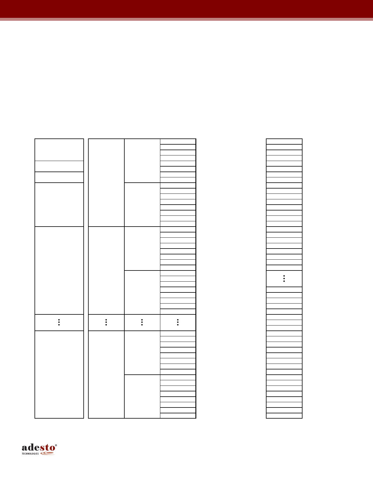
4. Memory Array
To provide the greatest flexibility, the memory array of the AT25DF041B can be erased in three levels of granularity
including a full chip erase. The size of the erase blocks is optimized for both code and data storage applications, allowing
both code and data segments to reside in their own erase regions. The Memory Architecture Diagram illustrates the
breakdown of each erase level.
Figure 4-1. Memory Architecture Diagram
Internal Sectoring for
Sector Protection
Function
16KB
(Sector 10)
8KB
(Sector 9)
8KB
(Sector 8)
32KB
(Sector 7)
64KB
(Sector 6)
Block Erase Detail
64KB
32KB
4KB
Block Erase
Block Erase
Block Erase
(D8h Command) (52h Command) (20h Command)
Block Address
Range
64KB
32KB
32KB
64KB
32KB
32KB
4KB 07F F F F h – 07F 000h
4KB 07E F F F h – 07E 000h
4KB 07DF F F h – 07D000h
4KB 07CF F F h – 07C000h
4KB 07BF F F h – 07B000h
4KB 07AF F F h – 07A000h
4KB 079F F F h – 079000h
4KB 078F F F h – 078000h
4KB 077F F F h – 077000h
4KB 076F F F h – 076000h
4KB 075F F F h – 075000h
4KB 074F F F h – 074000h
4KB 073F F F h – 073000h
4KB 072F F F h – 072000h
4KB 071F F F h – 071000h
4KB 070F F F h – 070000h
4KB 06F F F F h – 06F 000h
4KB 06E F F F h – 06E 000h
4KB 06DF F F h – 06D000h
4KB 06CF F F h – 06C000h
4KB 06BF F F h – 06B000h
4KB 06AF F F h – 06A000h
4KB 069F F F h – 069000h
4KB 068F F F h – 068000h
4KB 067F F F h – 067000h
4KB 066F F F h – 066000h
4KB 065F F F h – 065000h
4KB 064F F F h – 064000h
4KB 063F F F h – 063000h
4KB 062F F F h – 062000h
4KB 061F F F h – 061000h
4KB 060F F F h – 060000h
64KB
(Sector 0)
64KB
32KB
32KB
4KB 00F F F F h – 00F 000h
4KB 00E F F F h – 00E 000h
4KB 00DF F F h – 00D000h
4KB 00CF F F h – 00C000h
4KB 00BF F F h – 00B000h
4KB 00AF F F h – 00A000h
4KB 009F F F h – 009000h
4KB 008F F F h – 008000h
4KB 007F F F h – 007000h
4KB 006F F F h – 006000h
4KB 005F F F h – 005000h
4KB 004F F F h – 004000h
4KB 003F F F h – 003000h
4KB 002F F F h – 002000h
4KB 001F F F h – 001000h
4KB 000F F F h – 000000h
Page Program Detail
1-256 Byte
Page Program
(02h Command)
Page Address
Range
256 Bytes
256 Bytes
256 Bytes
256 Bytes
256 Bytes
256 Bytes
256 Bytes
256 Bytes
256 Bytes
256 Bytes
256 Bytes
256 Bytes
256 Bytes
256 Bytes
256 Bytes
256 Bytes
256 Bytes
256 Bytes
256 Bytes
256 Bytes
256 Bytes
256 Bytes
256 Bytes
256 Bytes
07FFFFh – 07FF00h
07FEFFh – 07FE00h
07F DF F h – 07F D00h
07FCFFh – 07FC00h
07FBFFh – 07FB00h
07F AF F h – 07F A00h
07F9FFh – 07F900h
07F8FFh – 07F800h
07F7FFh – 07F700h
07F6FFh – 07F600h
07F5FFh – 07F500h
07F4FFh – 07F400h
07F3FFh – 07F300h
07F2FFh – 07F200h
07F1FFh – 07F100h
07F0FFh – 07F000h
07EFFFh – 07EF00h
07EEFFh – 07EE00h
07E DF F h – 07E D00h
07ECFFh – 07EC00h
07EBFFh – 07EB00h
07E AF F h – 07E A00h
07E9FFh – 07E900h
07E8FFh – 07E800h
256 Bytes
256 Bytes
256 Bytes
256 Bytes
256 Bytes
256 Bytes
256 Bytes
256 Bytes
256 Bytes
256 Bytes
256 Bytes
256 Bytes
256 Bytes
256 Bytes
256 Bytes
256 Bytes
256 Bytes
256 Bytes
256 Bytes
256 Bytes
256 Bytes
256 Bytes
256 Bytes
256 Bytes
0017FFh – 001700h
0016FFh – 001600h
0015FFh – 001500h
0014FFh – 001400h
0013FFh – 001300h
0012FFh – 001200h
0011FFh – 001100h
0010FFh – 001000h
000FFFh – 000F00h
000EFFh – 000E00h
000DF F h – 000D00h
000CFFh – 000C00h
000BFFh – 000B00h
000AF F h – 000A00h
0009FFh – 000900h
0008FFh – 000800h
0007FFh – 000700h
0006FFh – 000600h
0005FFh – 000500h
0004FFh – 000400h
0003FFh – 000300h
0002FFh – 000200h
0001FFh – 000100h
0000FFh – 000000h
AT25DF041B
DS-25DF041B–040C–11/2015
5
5 Page 
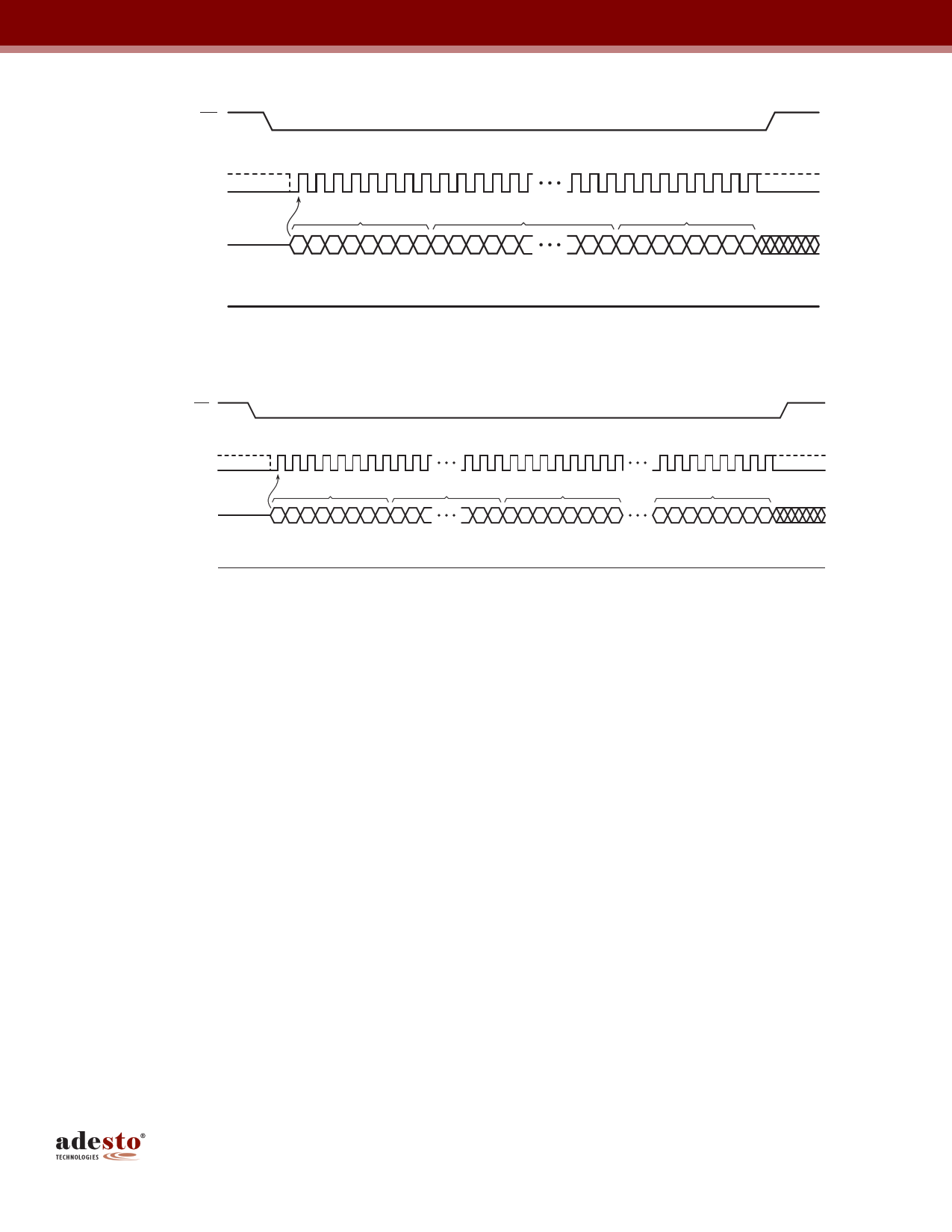
Figure 8-1. Byte Program
CS
SCK
SI
SO
0 1 2 3 4 5 6 7 8 9 10 11 12
29 30 31 32 33 34 35 36 37 38 39
OPCODE
ADDRESS BITS A23-A0
DATA IN
0 0 0 0 0 0 1 0AAAAAA
MSB
MSB
AAADDDDDDDD
MSB
HIGH-IMPEDANCE
Figure 8-2. Page Program
CS
SCK
SI
SO
0123456789
29 30 31 32 33 34 35 36 37 38 39
OPCODE
ADDRESS BITS A23-A0
DATA IN BYTE 1
0 0 0 0 0 0 1 0AAA
MSB
MSB
AAADDDDDDDD
MSB
HIGH-IMPEDANCE
DATA IN BYTE n
DDDDDDDD
MSB
8.2 Dual-Input Byte/Page Program
The Dual-Input Byte/Page Program command is similar to the standard Byte/Page Program command and can be used
to program anywhere from a single byte of data up to 256 bytes of data into previously erased memory locations. Unlike
the standard Byte/Page Program command, however, the Dual-Input Byte/Page Program command allows two bits of
data to be clocked into the device on every clock cycle rather than just one.
Before the Dual-Input Byte/Page Program command can be started, the Write Enable command must have been
previously issued to the device (see “Write Enable” on page 17) to set the Write Enable Latch (WEL) bit of the Status
Register to a Logical 1 state. To perform a Dual-Input Byte/Page Program command, an A2h opcode must be clocked
into the device followed by the three address bytes denoting the first location of the memory array to begin programming
at. After the address bytes have been clocked in, data can then be clocked into the device two bits at a time on both the
SO and SI pins.
The data is always input with the MSB of a byte first, and the MSB is always input on the SO pin. During the first clock
cycle, bit seven of the first data byte is input on the SO pin while bit six of the same data byte is input on the SI pin. During
the next clock cycle, bits five and four of the first data byte are input on the SO and SI pins, respectively. The sequence
continues with each byte of data being input after every four clock cycles. Like the standard Byte/Page Program
command, all data clocked into the device are stored in an internal buffer.
If the starting memory address denoted by A23-A0 does not fall on an even 256-byte page boundary (A7-A0 are not all
0), then special circumstances regarding which memory locations are to be programmed will apply. In this situation, any
data that are sent to the device that go beyond the end of the page will wrap around to the beginning of the same page.
In addition, if more than 256 bytes of data is sent to the device, then only the last 256 bytes sent will be latched into the
internal buffer.
Example: If the starting address denoted by A23-A0 is 0000FEh and three bytes of data are sent to the device, then
the first two bytes of data will be programmed at addresses 0000FEh and 0000FFh, while the last byte of
AT25DF041B
DS-25DF041B–040C–11/2015
11
11 Page | ||
| Páginas | Total 30 Páginas | |
| PDF Descargar | [ Datasheet AT25DF041B.PDF ] | |
Hoja de datos destacado
| Número de pieza | Descripción | Fabricantes |
| AT25DF041A | 4-megabit 2.7-volt Only Serial Firmware DataFlash Memory | ATMEL Corporation |
| AT25DF041A | 4-megabit 2.3-volt or 2.7-volt Minimum SPI Serial Flash Memory | Adesto |
| AT25DF041B | SPI Serial Flash Memory | Adesto |
| Número de pieza | Descripción | Fabricantes |
| SLA6805M | High Voltage 3 phase Motor Driver IC. |
Sanken |
| SDC1742 | 12- and 14-Bit Hybrid Synchro / Resolver-to-Digital Converters. |
Analog Devices |
|
DataSheet.es es una pagina web que funciona como un repositorio de manuales o hoja de datos de muchos de los productos más populares, |
| DataSheet.es | 2020 | Privacy Policy | Contacto | Buscar |
