|
|
|
PDF RT8109 Data sheet ( Hoja de datos )
| Número de pieza | RT8109 | |
| Descripción | 5V to 12V Single Synchronous Buck PWM Controller | |
| Fabricantes | Richtek | |
| Logotipo | ||
Hay una vista previa y un enlace de descarga de RT8109 (archivo pdf) en la parte inferior de esta página. Total 14 Páginas | ||
|
No Preview Available !
RT8109
5V to 12V Single Synchronous Buck PWM Controller with
Reference Input
General Description
The RT8109 is a single-phase synchronous buck PWM
DC-DC controller designed to drive two N-MOSFETs. It
provides a highly accurate, programmable output voltage
precisely regulated to low voltage requirement with an
internal 0.6V ±1% reference.
The RT8109 uses a single feedback loop voltage mode
PWM control for fast transient response. The high driving
capability makes it suitable for large output current
applications. An oscillator with fixed frequency 300kHz
reduces the component size of the external inductor and
capacitor for saving PCB board area and cost.
The RT8109 supports both tracking and stand-alone loop
control modes. Standalone mode is simple and tracking
mode provides better flexibility. The RT8109 also integrates
complete protection functions such as OCP, OVP, UVP
into WDFN-10L 3x3 package.
Ordering Information
RT8109
Package Type
QW : WDFN-10L 3x3 (W-Type)
Lead Plating System
G : Green (Halogen Free and Pb Free)
Note :
Richtek products are :
` RoHS compliant and compatible with the current require-
ments of IPC/JEDEC J-STD-020.
` Suitable for use in SnPb or Pb-free soldering processes.
Features
z Single IC Supply Voltage ( 5V to 12V).
z Drive Two N-MOSFETs
z Fixed Operating Frequency at 300kHz
z Voltage Mode PWM Control with External
Feedback Loop Compensation
z Over Current Protection by Sensing MOSFET RDS(ON)
z Dual Mode Regulation Control
`Standalone Mode (FB regulating to close to
internal reference 0.6V)
`Tracking Mode (FB following PI input)
z Power Good Indication
z On/Off Control
z Full 0 to 90% Duty Cycle
z RoHS Compliant and Halgen Free
Applications
z Mother Boards and Desktop Servers
z Graphic Cards
z Switching Power Supply
z Generic DC/DC Power Regulator
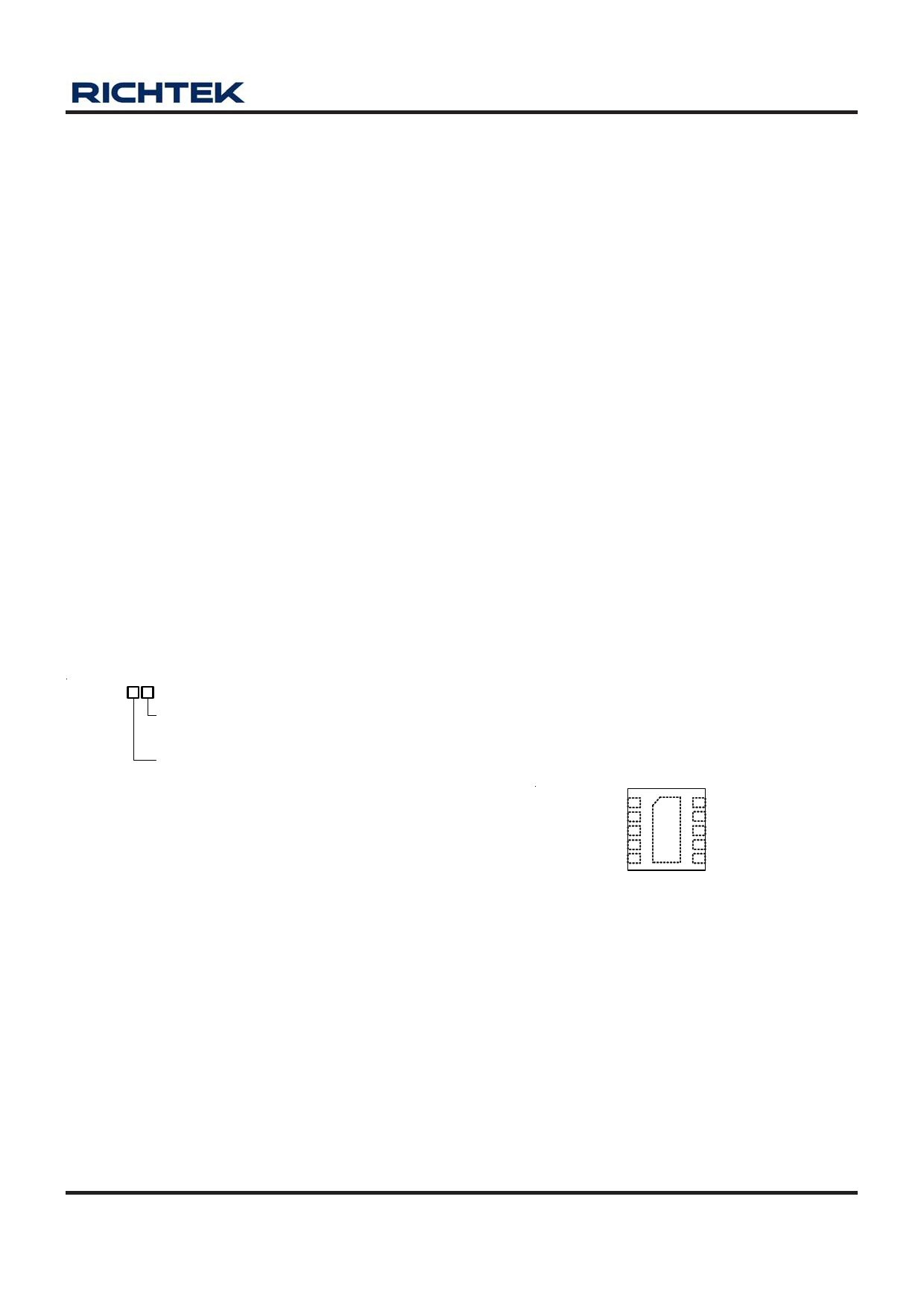
Pin Configurations
(TOP VIEW)
BOOT 1
UGATE 2
PHASE 3
GND 4
LGATE/OCSET 5
10 PI
9 PGOOD
8 COMP/SD
7 FB
11 6 VCC
WDFN-10L 3x3
Marking Information
For marking information, contact our sales representative
directly or through a Richtek distributor located in your
area.
DS8109-02 April 2011
www.richtek.com
1
1 page 
RT8109
Parameter
Symbol
Oscillator
PWM Frequency
Ramp Amplitude
FSW
ΔVOSC
Internal Reference (Standalone Mode)
Test Conditions
Min Typ Max Unit
250 300 350 kHz
-- 1.5 -- VP-P
Internal Reference Voltage
VR EF
0.594 0.6 0.606 V
External Reference (Tracking Mode)
Input Range
0.4 -- 3 V
Input Offset
−10 0
10 mV
PWM Controller
Open Loop DC Gain
AO
-- 88 -- dB
Gain Bandwidth
GBW
-- 15 -- MHz
Maximum Duty
DM AX
PWM Controller Gate Driver
-- 90 -- %
Upper Gate Source
Upper Gate Sink
Lower Gate Source
Lower Gate Sink
Protection
IUGATEsr VBOOT − VPHASE = 12V
1 1.2 --
RUGATEsk VUGATE − VPHASE = 0.1V, IUG = 50mA -- 2 --
ILGATEsr VCC = 12V
1 1.2 --
RLGATEsk VLGATE = 0.1V, ILG = 50mA
-- 1 --
A
Ω
A
Ω
Under Voltage Protection (UVP) VFB_UVP Sweep VFB
68 75 82 %
Over Voltage Protection
VFB_OVP Sweep VFB
115 125 130 %
LGATE OC Setting Current
IOCSET
22 25 28 μA
Over Temperature Protection
Soft Start Interval
TOTP
TSS
-- 170 -- °C
PI = 0.6V, Measure FB from 10% to
90%
1
3
5 ms
COMP/SD Shutdown Threshold VSD
-- -- 0.2 V
Note 1. Stresses beyond those listed under “Absolute Maximum Ratings” may cause permanent damage to the device.
These are stress ratings only, and functional operation of the device at these or any other conditions beyond those
indicated in the operational sections of the specifications is not implied. Exposure to absolute maximum rating
conditions for extended periods may affect device reliability.
Note 2. θJA is measured in the natural convection at TA = 25°C on a low effective single layer thermal conductivity test board of
JEDEC 51-3 thermal measurement standard.
Note 3. Devices are ESD sensitive. Handling precaution is recommended. The human body model is a 100pF capacitor
discharged through a 1.5kΩ resistor into each pin.
Note 4. The device is not guaranteed to function outside its operating conditions.
DS8109-02 April 2011
www.richtek.com
5
5 Page 
RT8109
LMIN
=
VIN − VOUT
FSW × k ×IOUT_Full Load
×
VOUT
VIN
where k is 0.2 to 0.3.
Input Capacitor Selection
Voltage rating and current rating are the key parameters in
selecting input capacitor. The voltage rating must be 1.25
times greater than the maximum input voltage to ensure
enough room for safe operation. Generally, input capacitor
has a voltage rating of 1.5 times greater than the maximum
input voltage is a conservatively safe design.
The input capacitor is used to supply the input RMS
current, which can be approximately calculated using the
following equation.
IRMS = IOUT ×
VOUT
VIN
× ⎛⎜⎝1−
VOUT
VIN
⎞⎟⎠
Refer to the manufacturer's databook for RMS current rating
to select proper capacitor. Use more than one capacitor
with low equivalent series resistance (ESR) in parallel to
form a capacitor bank is popular. Besides, placing ceramic
capacitor close to the drain of the high-side MOSFET is
helpful in reducing the input voltage ripple at heavy load.
Output Capacitor Selection
The output capacitor and the inductor form a low-pass filter
in the buck topology. The electrolytic capacitor is usually
used because it can provide large capacitance value. In
steady state condition, the output capacitor supplies only
AC ripple current to the load. The ripple current flows into/
out of the capacitor results in ripple voltage, which can be
determined using the following equation.
ΔVOUT_ESR = ΔIL x ESR
In addition, the output voltage ripple is also influenced by
the switching frequency and the capacitance value.
ΔVOUT_C
=
ΔIL
×
8
×
1
COUT
× FSW
The total output voltage ripple is the sum of VOUT_ESR and
VOUT_C.
If the specification for steady-state output voltage ripple is
known, the ESR can be determined using the above
equations.
Another parameter that has influence on the output voltage
undershoot is the equivalent series inductance (ESL). The
rapid change in load current results in di/dt during transient.
Therefore, ESL contributes to part of the voltage
undershoot. Use capacitor that has low ESL to obtain better
transient performance. Generally, use several capacitors
connected in parallel can have better transient performance
than use single capacitor for the same total ESR.
Unlike the electrolytic capacitor, the ceramic capacitor has
relatively low ESR and can reduce the voltage deviation
during load transient. However, the ceramic capacitor can
only provide low capacitance value. Therefore, use a mixed
combination of electrolytic capacitor and ceramic capacitor
can also have better transient performance.
Feedback Loop Compensation
Figure 4 shows the voltage mode control loop for a buck
converter. The control loop consists of the modulator, output
LC filter and the compensator. The modulator is composed
of the PWM comparator and power MOSFETs. The PWM
comparator compares the error amplifier EA output (COMP)
with the oscillator (OSC) sawtooth wave to generate a PWM
signal. The MOSFETs is then switched on and off
according to the duty cycle of the PWM signal. The voltage
presented at PHASE node is a square wave of 0V to Vin.
The PHASE voltage is filtered by the output filter LOUT and
COUT to produce output voltage VOUT, which is fedback to
the inverting input of the error amplifier. The output voltage
is then regulated according to the reference voltage VREF.
In order to achieve fast transient response and accurate
output regulation, an adequate compensator design is
necessary. The goal of the compensation network is to
provide adequate phase margin (greater than 45 degrees)
and the highest 0dB crossing frequency. It is also
recommended to manipulate loop frequency response that
its gain crosses over 0dB at a slope of −20dB/dec.
DS8109-02 April 2011
www.richtek.com
11
11 Page | ||
| Páginas | Total 14 Páginas | |
| PDF Descargar | [ Datasheet RT8109.PDF ] | |
Hoja de datos destacado
| Número de pieza | Descripción | Fabricantes |
| RT810 | Diode ( Rectifier ) | American Microsemiconductor |
| RT810 | AUTOMOTIVE BRIDGE RECTIFIERS | Leshan Radio Company |
| RT8100 | Synchronous buck PWM DC/DC | Richtek |
| RT8100A | Synchronous buck PWM DC/DC | Richtek Technology Corporation |
| Número de pieza | Descripción | Fabricantes |
| SLA6805M | High Voltage 3 phase Motor Driver IC. |
Sanken |
| SDC1742 | 12- and 14-Bit Hybrid Synchro / Resolver-to-Digital Converters. |
Analog Devices |
|
DataSheet.es es una pagina web que funciona como un repositorio de manuales o hoja de datos de muchos de los productos más populares, |
| DataSheet.es | 2020 | Privacy Policy | Contacto | Buscar |