|
|
|
PDF ICS307-03 Data sheet ( Hoja de datos )
| Número de pieza | ICS307-03 | |
| Descripción | SERIALLY PROGRAMMABLE CLOCK SOURCE | |
| Fabricantes | Integrated Circuit Systems | |
| Logotipo | ||
Hay una vista previa y un enlace de descarga de ICS307-03 (archivo pdf) en la parte inferior de esta página. Total 12 Páginas | ||
|
No Preview Available !
ICS307-03
SERIALLY PROGRAMMABLE CLOCK SOURCE
Description
The ICS307-03 is a dynamic, serially programmable
clock source which is flexible and takes up minimal
board space. Output frequencies are programmed via
a 3-wire SPI port.
An advanced PLL coupled to an array of configurable
output dividers and three outputs allows low-jitter
generation of frequencies from 200 Hz to 270 MHz.
The device can be reprogrammed during operation,
making it ideal for applications where many different
frequencies are required, or where the output
frequency must be determined at run time. Glitch-free
frequency transitions, where the clock period changes
slightly over many cycles, are possible.
Features
• Crystal or clock reference input
• 3.3 V CMOS outputs
• Three outputs can be individually configured or shut
off
• Small 16-pin TSSOP package
• Reprogrammable during operation
• 3-wire SPI serial interface
• Glitch-free output frequency switching
• User selectable charge pump current and damping
resistor
• Power-down control via hardware pin or software
control bit
• Programming word can be generated by ICS
VersaClock II Software
• Directly programmable via VersaClock II Software
and a Windows PC parallel port
• Available in Pb (lead) free package
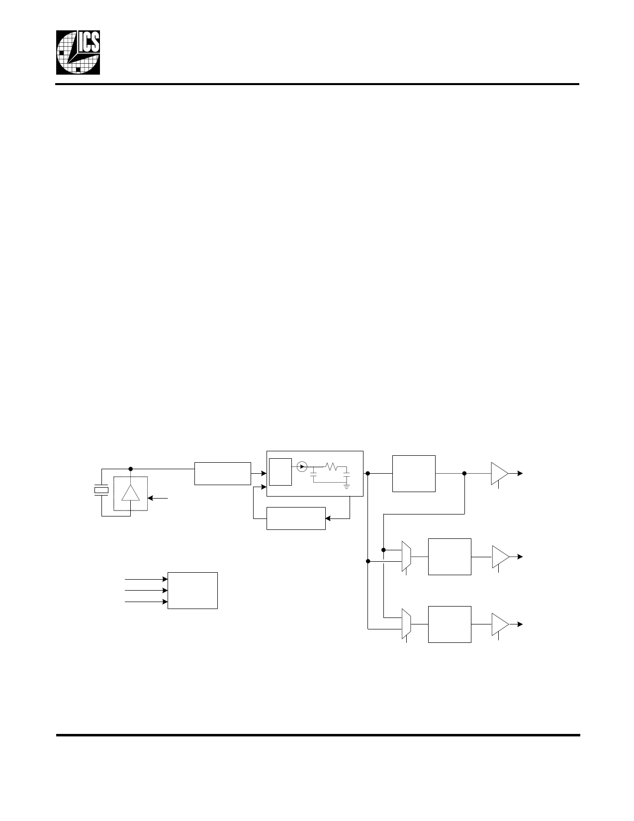
Block Diagram
(Table 1)
X1
REF Divide
1-2055
[Bit 122]
X2
Charge Pump
(Table 3)
CP 11pF
Resistor
(Table 4)
300
pF
VCO DIVIDE
12-2055
(Table 2)
DIN
CS
SCLK
Programming
Register
(132 bits)
Divider
2 - 8232
(Table 5)
[Bit 110]
CLK1
1
0
[Bit 123]
Divider
2 - 34
(Table 6)
[Bit 111]
CLK2
1
0
[Bit 124]
Divider
2 - 34
(Table 7)
[Bit 129]
CLK3
MDS 307-03 C
1
Revision 101705
Integrated Circuit Systems ● 525 Race Street, San Jose, CA 95126 ● tel (408) 297-1201 ● www.icst.com
1 page 
ICS307-03
SERIALLY PROGRAMMABLE CLOCK SOURCE
Table 5. Output Divider for Output 1
Divide
Bits
Value 109 108 107 106 105 104 103 102 101 100 99 98 97 96 95 Rule
2 X X X X X X X X X X X0000
3 X X X X X X X X X X X0001
4 X X X X X X X X X X X1000
5 X X X X X X X X X X XX0 1 0
6 X X X X X X X X X X X1001
7 X X X X X X X X X X 00011
8 X X X X X X X 1 1 1 0 1 1 0 0 apply Rule from Divide Values 14-37
9 X X X X X X X X X X 10011
10 X X X X X X X 1 1 0 1 1 1 0 0 apply Rule from Divide Values 14-37
11 X X X X X X X X X X 0 1 0 1 1
12 X X X X X X X 1 1 0 0 1 1 0 0 apply Rule from Divide Values 14-37
13 X X X X X X X X X X 1 1 0 1 1
14 X X X X X X X 1 0 1 1 1 1 0 0 subtract 6 from the desired
15 X X X X X X X 1 0 1 1 0 1 0 0 divide value, convert to binary,
invert, and apply to bits 102..98
set bits [97..95] = 100
36 X X X X X X X 0 0 0 0 1 1 0 0
37 X X X X X X X 0 0 0 0 0 1 0 0
38 0 0 0 0 1 0 0 0 0 0 0 1 1 0 1 output divide =
39 0 0 0 0 1 0 0 0 0 0 0 1 1 0 1 ((([109..101]+3)*2)+[98])*2^[100
(increments of 1)
set bits [95..97] = 101 †
1029 1 1 1 1 1 1 1 1 1 0 0 0 1 0 1 († this Rule applies to Divide
1030 0 1 1 1 1 1 1 1 0 0 1 0 1 0 1 Values 38-8232)
1032 0 1 1 1 1 1 1 1 1 0 1 1 1 0 1
(increments of 2)
2056 1 1 1 1 1 1 1 1 1 0 1 1 1 0 1
2058 1 1 1 1 1 1 1 1 1 0 1 0 1 0 1
2060 0 1 1 1 1 1 1 1 0 1 0 0 1 0 1
2064 0 1 1 1 1 1 1 1 1 1 0 1 1 0 1
(increments of 4)
4112 1 1 1 1 1 1 1 1 1 1 0 1 1 0 1
4116 1 1 1 1 1 1 1 1 1 1 0 0 1 0 1
4120 0 1 1 1 1 1 1 1 0 1 1 0 1 0 1
4128 0 1 1 1 1 1 1 1 1 1 1 1 1 0 1
(increments of 8)
8224 1 1 1 1 1 1 1 1 1 1 1 1 1 0 1
8232 1 1 1 1 1 1 1 1 1 1 1 0 1 0 1
MDS 307-03 C
5
Revision 101705
Integrated Circuit Systems ● 525 Race Street, San Jose, CA 95126 ● tel (408) 297-1201 ● www.icst.com
5 Page 
ICS307-03
SERIALLY PROGRAMMABLE CLOCK SOURCE
AC Electrical Characteristics
VDD = 3.3 V ±5%, Ambient Temperature 0 to +70° C, unless stated otherwise
Parameter
Symbol
Conditions
Min.
Input Frequency
FIN Fundamental crystal
Clock
3
0.1
Clock Output Frequency
FOUT
5 pF load
15 pF load
0.0002
0.0002
Output Clock Rise/Fall Time
Output Clock Duty Cycle
tR, tF
20 to 80% (5 pF load)
Output Divides <> 3
45
Output Divide = 3
40
Frequency Transition time
STROBE high to CLK
out
One Sigma Clock Period Jitter
Note 2
Maximum Absolute Jitter
tja Deviation from mean,
Note 2
VCO Frequency
Divider 1 Input
VCOF
Output divider 1 = 2
(5 pF load)
Output divider 1 = 2
(15 pF load)
Output divider 1 = 3
(5 pF load)
Output divider 1 = 3
(15 pF load)
Output divider 1 = 38
~ 1029
All other Output
Divider 1 values
Divider 2 and 3 Inputs
Output divider 2, 3 = 2
(5 pF load)
Output divider 2, 3 = 2
(15 pF load)
Output divider 2, 3=12
Output divider 2, 3 =
16, 24, 28 and 32
All other Output
Divider 2 & 3 values
Note 1: Measured with 15 pF load.
Note 2: Jitter performance will change depending on configuration settings.
Typ.
1.5
49-51
3
50
±120
100
Max.
27
300
270
200
55
60
10
730
540
400
720
600
570
730
540
400
440
500
730
Units
MHz
MHz
MHz
MHz
ns
%
%
ms
ps
ps
MHz
MHz
MHz
MHz
MHz
MHz
MHz
MHz
MHz
MHz
MHz
MHz
MDS 307-03 C
11
Revision 101705
Integrated Circuit Systems ● 525 Race Street, San Jose, CA 95126 ● tel (408) 297-1201 ● www.icst.com
11 Page | ||
| Páginas | Total 12 Páginas | |
| PDF Descargar | [ Datasheet ICS307-03.PDF ] | |
Hoja de datos destacado
| Número de pieza | Descripción | Fabricantes |
| ICS307-01 | SERIALLY PROGRAMMABLE CLOCK SOURCE | IDT |
| ICS307-01 | SERIALLY PROGRAMMABLE CLOCK SOURCE | Integrated Circuit Systems |
| ICS307-02 | SERIALLY PROGRAMMABLE CLOCK SOURCE | IDT |
| ICS307-02 | SERIALLY PROGRAMMABLE CLOCK SOURCE | Integrated Circuit Systems |
| Número de pieza | Descripción | Fabricantes |
| SLA6805M | High Voltage 3 phase Motor Driver IC. |
Sanken |
| SDC1742 | 12- and 14-Bit Hybrid Synchro / Resolver-to-Digital Converters. |
Analog Devices |
|
DataSheet.es es una pagina web que funciona como un repositorio de manuales o hoja de datos de muchos de los productos más populares, |
| DataSheet.es | 2020 | Privacy Policy | Contacto | Buscar |