|
|
|
PDF LM2507 Data sheet ( Hoja de datos )
| Número de pieza | LM2507 | |
| Descripción | Low Power Mobile Pixel Link (MPL) Level 0 / 16-bit CPU Display interface Serializer and Deserializer | |
| Fabricantes | National Semiconductor | |
| Logotipo | ||
Hay una vista previa y un enlace de descarga de LM2507 (archivo pdf) en la parte inferior de esta página. Total 22 Páginas | ||
|
No Preview Available !
August 2006
LM2507
Low Power Mobile Pixel Link (MPL) Level 0, 16-bit CPU
Display interface Serializer and Deserializer
General Description
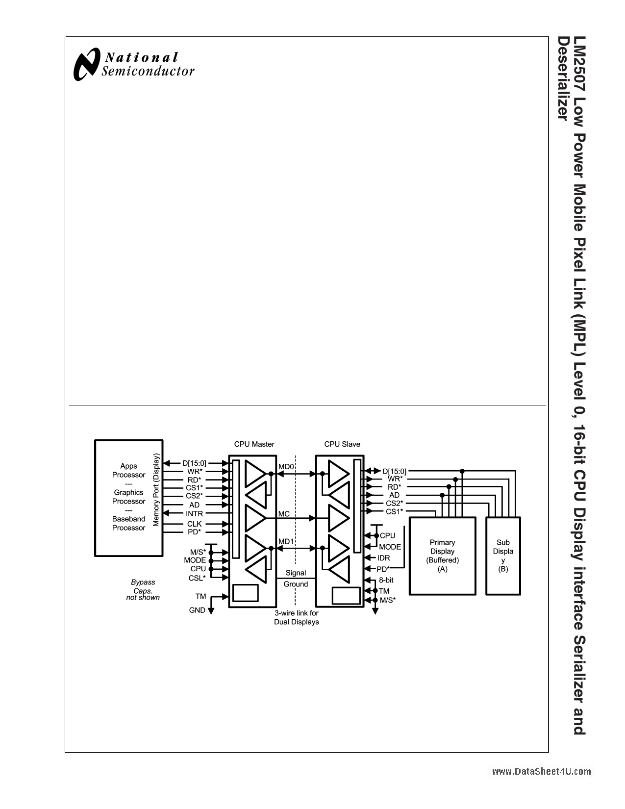
The LM2507 device adapts i80 CPU style display interfaces
to the Mobile Pixel Link (MPL) Level zero serial link. When
using smart CPU type interfaces, two chip selects support a
main and sub display. A mode pin configures the device as a
Master (MST) or Slave (SLV) so the same chip can be used
on both sides of the interface.
The interconnect is reduced from 21 signals to only 3 active
signals with the LM2507 chipset easing flex interconnect
design, size constraints and cost.
The LM2507 in MST mode resides beside an application,
graphics or baseband processor and translates a parallel
bus from LVCMOS levels to serial Mobile Pixel Link levels for
transmission over a flex cable (or coax) and PCB traces to
the SLV located near the display module(s).
When the Power_Down (PD*) input is asserted on the Mas-
ter, the MDn and MC line drivers are powered down to save
current. The Slave is controlled by a separate Power_Down
input.
The LM2507 implements the physical layer of the MPL Level
0 Standard (MPL-0) and a 150 µA IB current (Class 0).
Features
n CPU Display Interface support up to
800 x 300 1⁄2SVGA formats
n Dual displays supported – CS1* & CS2*
n MPL-Level 0 Physical Layer using two data and one
clock signal
n Low Power Consumption
n Pinout mirroring enables straight through layout with
minimal vias
n Level translation between host and display
n Link power down mode reduces quiescent power
under < 10 µA
n 1.74V to 2.0V core / analog supply voltage range
n 1.74V to 3.0V I/O supply voltage range
System Benefits
n Small Interface
n Low Power
n Low EMI
n Intrinsic Level Translation
Typical Application Diagram - CPU Mode
www.DataSheet4U.com
© 2006 National Semiconductor Corporation DS201860
20186001
www.national.com
1 page 
Electrical Characteristics (Continued)
Over recommended operating supply and temperature ranges unless otherwise specified. (Notes 2, 3)
Symbol
Parameter
Conditions
Min Typ
SUPPLY CURRENT
IDDZ
Supply Current — Disable
TA = 25˚C
Power Down Modes
MST
PD* = L
SLV
PD* = L
VDDIO
VDD/VDDA
VDDIO
VDD/VDDA
<1
<1
<1
<1
Switching Characteristics
Over recommended operating supply and temperature ranges unless otherwise specified. (Note 2)
Symbol
Parameter
Conditions
Min Typ
PARALLEL BUS TIMING See
tSET
tHOLD
tRISE
tFALL
Set Up Time
Hold Time
Rise Time
Fall Time
5
5
Edge sensitive
outputs only,
(Note 6)
CL = 15 pF,
Figure 2
VDDIO = 1.74V
VDDIO = 3.0V
VDDIO = 1.74V
VDDIO = 3.0V
7
3
7
2
SERIAL BUS TIMING
tDVBC
Serial Data Valid before
Clock (Set Time)
SLV Input
Figure 1
MC = 80MHz
(Note 9)
1.5
tDVAC
Serial Data Valid after
Clock (Hold Time)
1.5
POWER UP TIMING
t0 MST PLL Lock Counter
4,096
t1 MC Pulse Width Low
180
t2 MC Pulse Width High
180
t3 MC H-L to Idle State
180
MPL POWER OFF TIMING
tPAZ Disable Time to Power
Down
(Note 8)
Max
2
2.2
2
2.2
Max
15.5
6.5
15.5
6
2
Units
µA
µA
µA
µA
Units
ns
ns
ns
ns
ns
ns
ns
ns
CLK
cycles
MC
cycles
MC
cycles
MC
cycles
ms
Recommended Input Timing Requirements
Over recommended operating supply and temperature ranges unless otherwise specified. (Note 2)
Symbol
Parameter
Conditions
Min Typ
MASTER REFERENCE CLOCK (CLK)
f Clock Frequency
3
tCP Clock Period
CLKDC
Clock Duty Cycle
wwtwT .DataSheeCTt4ilmoUce.kcs/oD(mRatisaeTorar nFsaitlilo, n
10%–90%)
(Note 7)
50
30 50
2
Max
20
333
70
Units
MHz
ns
%
ns
Note 1: “Absolute Maximum Ratings” are those values beyond which the safety of the device cannot be guaranteed. They are not meant to imply that the device
should be operated at these limits. The tables of “Electrical Characteristics” specify conditions for device operation.
Note 2: Typical values are given for VDDIO = 1.8V and VDD = VDDA = 1.8V and TA = 25˚C.
Note 3: Current into a device pin is defined as positive. Current out of device pins is defined as negative. Voltages are referenced to Ground unless otherwise
specified.
Note 4: MPL Current Threshold is set to be 3XIB by the MPL start up Sequence - this is a functional specification only.
5 www.national.com
5 Page 
Functional Description (Continued)
FIGURE 11. WRITE — i80 CPU Interface
TABLE 2. WRITE — i80 CPU Interface Parameters
No. Parameter
T1 MasterIN Data Setup before Write* High
T2 MasterIN Data Hold after Write* High
T3 MasterIN Write* Cycle Rate
T4 Master Master Latency
T5 Slave Slave Latency
T6 SlaveOUT Data Valid before Write* High-to-Low
T7 SlaveOUT WR* Pulse Width Low, 16-bit mode
T8 SlaveOUT Data Valid before Write* Low-to-High
T9 SlaveOUT Data Valid after Write* Low-to-High
Min Typ
3.5
2.5
6
7
8
1
3
4
1
20186012
Max
Units
ns
ns
MC Cycles
MC Cycles
MC Cycles
MC Cycles
MC Cycles
MC Cycles
MC Cycles
www.DataSheet4U.com
11 www.national.com
11 Page | ||
| Páginas | Total 22 Páginas | |
| PDF Descargar | [ Datasheet LM2507.PDF ] | |
Hoja de datos destacado
| Número de pieza | Descripción | Fabricantes |
| LM250 | ADJUSTABLE VOLTAGE REGULATORS THREE-TERMINAL 3 A | STMicroelectronics |
| LM25005 | LM25005 42V 2.5A Step-Down Switching Regulator (Rev. C) | Texas Instruments |
| LM25005 | STEP-DOWN SWITCHING REGULATOR | National Semiconductor |
| LM25007 | LM25007 42V 0.5A Step-Down Switching Regulator (Rev. C) | Texas Instruments |
| Número de pieza | Descripción | Fabricantes |
| SLA6805M | High Voltage 3 phase Motor Driver IC. |
Sanken |
| SDC1742 | 12- and 14-Bit Hybrid Synchro / Resolver-to-Digital Converters. |
Analog Devices |
|
DataSheet.es es una pagina web que funciona como un repositorio de manuales o hoja de datos de muchos de los productos más populares, |
| DataSheet.es | 2020 | Privacy Policy | Contacto | Buscar |