|
|
|
PDF ISL6174 Data sheet ( Hoja de datos )
| Número de pieza | ISL6174 | |
| Descripción | Dual Low Voltage Circuit Breaker | |
| Fabricantes | Intersil Corporation | |
| Logotipo | ||
Hay una vista previa y un enlace de descarga de ISL6174 (archivo pdf) en la parte inferior de esta página. Total 16 Páginas | ||
|
No Preview Available !
®
Data Sheet
December 19, 2008
ISL6174
www.DataSheet4U.com
FN6830.0
Dual Low Voltage Circuit Breaker
This IC targets dual voltage hot swap applications across the
+2.5V to +3.3V (nominal) bias supply voltage range with a
second lower voltage rail down to less than 1V where a circuit
breaker response to an over current event is preferred.
It features a charge pump for driving external N-Channel
MOSFETs, accurate programmable circuit breaker current
thresholds and delay output undervoltage monitoring and
reporting and adjustable soft-start.
The circuit breaker current level (ICB) for each rail is set by
two external resistors, and for each rail a delay (tCB) is set by
an external capacitor on the TCB pin. After tCB has expired,
the IC then quickly pulls down the associated GATE(s)
output turning off its external FET(s).
Ordering Information
PART NUMBER PART
(Note)
MARKING
TEMP.
RANGE
(°C)
PACKAGE PKG.
(Pb-Free) DWG. #
ISL6174IRZ* ISL6174 IRZ -40 to +85 28 Ld 5x5 QFN L28.5x5
ISL617XEVAL1Z Evaluation Platform
*Add “-T” suffix for tape and reel. Please refer to TB347 for details on
reel specifications.
NOTE: These Intersil Pb-free plastic packaged products employ
special Pb-free material sets, molding compounds/die attach materials,
and 100% matte tin plate plus anneal (e3 termination finish, which is
RoHS compliant and compatible with both SnPb and Pb-free soldering
operations). Intersil Pb-free products are MSL classified at Pb-free
peak reflow temperatures that meet or exceed the Pb-free
requirements of IPC/JEDEC J STD-020.
Pinout
ISL6174
(28 LD QFN)
TOP VIEW
28 27 26 25 24 23 22
SNS1 1
21 SNS2
VO1 2
20 VO2
SS1 3
19 SS2
GT1 4
18 GT2
FLT1 5
17 FLT2
PG1 6
16 PG2
TCB1 7
15 TCB2
8 9 10 11 12 13 14
Features
• Fast Circuit Breaker Quickly Responds to Overcurrent
Fault Conditions
• Less than 1µs Response Time to Dead Short
• Programmable Circuit Breaker Level and Delay
• Two Levels of Overcurrent Detection Provide Fast
Response to Varying Fault Conditions
• Overcurrent Circuit Breaker and Fault Isolation Functions
• Adjustable Circuit Breaker Threshold as Low as 20mV
• Adjustable Voltage Ramp-up for In-Rush Protection
During Turn-On
• Rail Independent Control, Monitoring and Reporting I/O
• Dual Supply Hot Swap Power Distribution Control to <1V
• Charge Pump Allows the Use of N-Channel MOSFETs
• QFN Package:
- Compliant to JEDEC PUB95 MO-220
QFN - Quad Flat No Leads - Package Outline
- Near Chip Scale Package Footprint, Which Improves
PCB Efficiency and has a Thinner Profile
• Pb-Free (RoHS Compliant)
Applications
• Power Supply Sequencing, Distribution and Control
• Hot Swap / Electronic Circuit Breaker Circuits
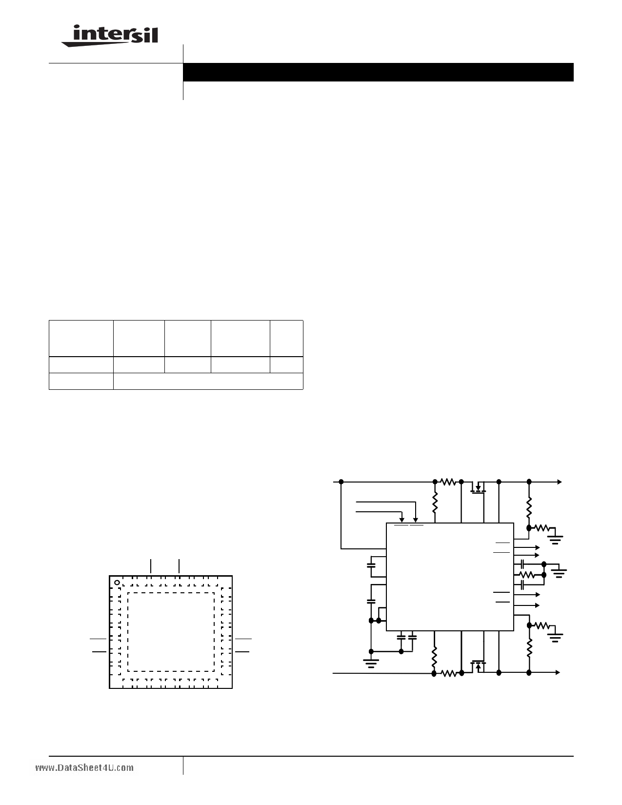
V1(IN)
RSNS1
V1(OUT)
EN1 EN2 VS1 SNS1 GT1 VO1
UV1
BIAS
CPQ+
PG1
FLT1
SS1
CPQ-
CPVDD
ISL6174
OCREF
SS2
FLT2
PGND
PG2
GND
UV2
TCB1 TCB2 VS2 SNS2 GT2 VO2
V2(IN)
RSNS2
FIGURE 1. TYPICAL APPLICATION
V2(OUT)
1 CAUTION: These devices are sensitive to electrostatic discharge; follow proper IC Handling Procedures.
1-888-INTERSIL or 1-888-468-3774 | Intersil (and design) is a registered trademark of Intersil Americas Inc.
Copyright Intersil Americas Inc. 2008. All Rights Reserved
All other trademarks mentioned are the property of their respective owners.
1 page 
ISL6174
Absolute Maximum Ratings
VBIAS . . . . . . . . . . . . . . . . . . . . . . . . . . . . . . . . . . . . . . . . . . . +5.5V
GTx, CPQ+ . . . . . . . . . . . . . . . . . . . . . . . . . . . . . . . . . -0.3V to +12V
ENx, SNSx, PGx, FLTx, VSx, TCBx, UVx,
SSx, CPQ-, CPVDD. . . . . . . . . . . . . . . . . . . . . . . . -0.3V to 5.5VDC
Output Current . . . . . . . . . . . . . . . . . . . . . . . Short Circuit Protected
Thermal Information
www.DataSheet4U.com
Thermal Resistance (Typical, Notes 1, 4) θJA (°C/W) θJC (°C/W)
5x5 QFN Package . . . . . . . . . . . . . . . .
42
12.5
Maximum Storage Temperature Range . . . . . . . . . .-65°C to +150°C
For recommended soldering conditions, see Tech Brief TB389.
(QFN - Leads Only)
Pb-Free Reflow Profile. . . . . . . . . . . . . . . . . . . . . . . . .see link below
http://www.intersil.com/pbfree/Pb-FreeReflow.asp
Operating Conditions
VBIAS / VIN1 Supply Voltage Range. . . . . . . . . . . +2.25V to +3.63V
Temperature Range (TA)
-40°C to +85°C
CAUTION: Do not operate at or near the maximum ratings listed for extended periods of time. Exposure to such conditions may adversely impact product reliability and
result in failures not covered by warranty.
NOTES:
1. θJA is measured in free air with the component mounted on a high effective thermal conductivity test board with “direct attach” features. See
Tech Brief TB379.
2. All voltages are relative to GND, unless otherwise specified.
3. 1V (min) on the BIAS pin required for FLT to be valid.
4. For θJC, the “case temp” location is the center of the exposed metal pad on the package underside..
Electrical Specifications
VDD = 2.5V to +3.3V, VS = 1V,TA = TJ = -40°C to +85°C, Unless Otherwise Specified. Parameters with MIN
and/or MAX limits are 100% tested at +25°C, unless otherwise specified.
Temperature limits established by characterization and are not production tested.
PARAMETER
SYMBOL
TEST CONDITIONS
MIN TYP MAX UNIT
CIRCUIT BREAKER CONTROL
ISET Current
Over Current Comparator Offset Voltage
Circuit Breaker Threshold Voltage
TCB Threshold Voltage
TCB Charging Current
TCB Default Delay
GATE DRIVE
ISET
Vio
VCRVTH
VCT_Vth
ICT
TCT
ROCREF = 14.7kΩ
VVS - VSNS with IOUT = 0A
VVS - VSNS at FLT assertion,
RISET = 1.0k, ISET = 20µA
Peak Voltage
TCB = Open
19
-1.25
1.128
9
20
-0.05
19.7
1.178
10
3
21
1.25
1.202
11
µA
mV
mV
V
µA
µs
GATE Response Time from WOC (Open) pd_woc_open GATE open
3 ns
100mV of overdrive on the WOC
comparator
GATE Response Time from WOC
pd_woc_load GATE = 1nF
100 ns
(Loaded)
100mV of overdrive on the WOC
comparator
GATE Turn-On Current
GATE Turn-Off Current
IGATE_on
GATE = 2V, VVS = 2V, VSNS = 2.1V
21
24
27 µA
IGATE_off
OC or WOC Turn-off Gate Current
100
mA
GATE Voltage
VGATE
Bias = 2.5V (Figure 5, 6)
2.1 < Bias < 2.5 (Figure 5, 6)
8.2 8.8 9.3 V
7V
BIAS
Supply Current
POR Rising Threshold
IBIAS
VBIAS = 3.3V
VIN_POR_L2H
6 9.3 12 mA
1.85 2.02 2.12
V
POR Falling Threshold
VIN_POR_H2L
1.80 1.98 2.10
V
POR Threshold Hysteresis
VIN_POR_HYS
5 33
mV
5 FN6830.0
December 19, 2008
5 Page 
ISL6174
LOAD CURRENT CARRYING
TRACES
CURRENT
SENSE
TRACES
RSNS
FIGURE 17. RECOMMENDED CURRENT SENSE RESISTOR
PCB LAYOUT
Current Set Resistor (RSET)
This resistor sets the threshold for the Circuit Breaker
comparator in conjunction with RSNS. Once RSNS has been
selected, use Equation 1 to calculate RSET. Use 20µA for
ISET in a typical application.
Reference Current Set Resistor (RREF)
This resistor sets up the current in the internal current
source, IREF/4, shown in Figure 2 for the comparators. The
voltage at the OCREF pin is the same as the internal
bandgap reference. The current (IREF) flowing through this
resistor is simply:
IREF = 1.178/RREF
This current, IREF, should be set at 80µA to force 20µA in the
internal current source as shown in Figure 2, because of the
4:1 current mirror. This equates to the resistor value of
14.7k.
Selection of Rs1 and Rs2
These resistors set the UV detect point. The UV comparator
detects the undervoltage condition when it sees the voltage
at UV pin drop below 0.633V. The resistor divider values
should be selected accordingly.
Charge Pump Capacitor Selection (CP and CV)
CP is the “flying cap” and CV is the smoothing cap of the
charge pump, which operates at 450kHz set internally. The
output resistance of the charge pump, which affects the
regulation, is dependent on the CP value and its ESR,
charge-pump switch resistance, and the frequency and ESR
of the smoothing cap, CV.
It is recommended that CP be kept within 0.022µF
(minimum) to 0.1µF (maximum) range. Only ceramic
capacitors are recommended. Use 0.1µF cap if CPVDD
output is expected to power an external circuit, in which case
the current draw from CPVDD must be kept below 10mA.
CV should at least be 0.47µF (ceramic only). Higher values
may be used if low ripple performance is desired.
Time-out Capacitor Selectionw(CwwT).DataSheet4U.com
This capacitor determines the current regulation delay
period. As shown in Figure 2, when the voltage across this
capacitor exceeds 1.178V, the time-out comparator detects it
and the gate voltage is pulled to 0V thus shutting down the
channel. An internal 10µA current source charges this
capacitor. Hence, the value of this capacitor is determined by
Equation 2.
CT= (10μA • TOUT) ⁄ 1.178
(EQ. 2)
Where,
TOUT = Desired time-out period.
Soft-Start Capacitor Selection (CSS)
The rate of change of voltage (dv/dt) on this capacitor, which
is determined by the internal 10µA current source, is the
same as that on the output load capacitance. Hence, the
value of this capacitor directly controls the inrush current
amplitude during hot swap operation.
CSS= CO • (10μA ⁄ IINRUSH)
(EQ. 3)
Where,
CO = Load Capacitance
IINRUSH = Desired Inrush Current
IINRUSH is the sum of the DC steady-state load current and
the load capacitance charging current. If the DC steady-state
load remains disabled until after the soft-start period expires
(PGx could be used as a load enable signal, for example),
then only the capacitor charging current should be used as
IINRUSH. The Css value should always be more than (1/2.4)
of that of Ciss of the MOSFET to ensure proper soft-start
operation. This is because the Ciss is charged from 24µA
current source, whereas the Css gets charged from a 10µA
current source (Figure 15). In order to make sure both VSS
and VO track during the soft-start, this condition is
necessary.
ISL6174 Evaluation Platform
The ISL617XEVAL1Z is the primary evaluation board for this
IC. For the BOM, schematic and photograph, see the “BOM
for ISL617XEVAL1Z Board and Schematic” on page 15.
The evaluation board has been designed with a typical
application in mind and with accessibility to all the featured
pins to enable a user to understand and verify these features
of the IC. The two circuit breaker levels are programmed to
2.2A for each input rail but they can easily be scaled up or
down by adjusting some component values.
There are two input voltages, one for each channel that are
switched by a dual N-Channel MOSFET (Q1) to the output
connectors.
11 FN6830.0
December 19, 2008
11 Page | ||
| Páginas | Total 16 Páginas | |
| PDF Descargar | [ Datasheet ISL6174.PDF ] | |
Hoja de datos destacado
| Número de pieza | Descripción | Fabricantes |
| ISL6172 | Dual Low Voltage Hot Swap Controller | Intersil Corporation |
| ISL6172DRZA | Dual Low Voltage Hot Swap Controller | Intersil Corporation |
| ISL6172DRZA-T | Dual Low Voltage Hot Swap Controller | Intersil Corporation |
| ISL6173 | Dual Low Voltage Hot Swap Controller | Intersil Corporation |
| Número de pieza | Descripción | Fabricantes |
| SLA6805M | High Voltage 3 phase Motor Driver IC. |
Sanken |
| SDC1742 | 12- and 14-Bit Hybrid Synchro / Resolver-to-Digital Converters. |
Analog Devices |
|
DataSheet.es es una pagina web que funciona como un repositorio de manuales o hoja de datos de muchos de los productos más populares, |
| DataSheet.es | 2020 | Privacy Policy | Contacto | Buscar |