|
|
|
PDF SC486 Data sheet ( Hoja de datos )
| Número de pieza | SC486 | |
| Descripción | Complete DDR1/2/3 Memory Power Supply | |
| Fabricantes | Semtech Corporation | |
| Logotipo | ||
Hay una vista previa y un enlace de descarga de SC486 (archivo pdf) en la parte inferior de esta página. Total 26 Páginas | ||
|
No Preview Available !
POWER MANAGEMENT
Description
The SC486 is a combination switching regulator and linear
source/sink regulator intended for DDR1/2/3 memory
systems. The switching regulator is used to generate the
supply voltage, VDDQ, for the memory system. It is a
pseudo-fixed frequency constant on-time controller
designed for high efficiency, superior DC accuracy, and
fast transient response. The linear source/sink regulator
is used to generate the memory termination voltage, VTT,
with the ability to source and sink a 3A peak current.
www.DataFSoherett4hUe.coVmDDQ regulator, the switching frequency is
constant until a step in load or line voltage occurs at
which time the pulse density, i.e. frequency, will increase
or decrease to counter the transient change in output or
input voltage. After the transient, the frequency will return
to steady-state operation. At lighter loads, the selectable
Power-Save Mode enables the PWM converter to reduce
its switching frequency and improve efficiency. The
integrated gate drivers feature adaptive shoot-through
protection and soft-switching.
For the VTT regulator, the output voltage tracks VREF,
which is ½ VDDQ to provide an accurate termination
voltage. The VTT output is generated from a 1.2V to VDDQ
input by a linear source/sink regulator which is designed
for high DC accuracy, fast transient response, and low
external component count. Additional features include
cycle-by-cycle current limiting, digital soft-start, power
good (all VDDQ only) and over-voltage and under-voltage
protection (VDDQ and VTT). All 3 outputs (VDDQ, VTT and
REF) are actively discharged when VDDQ is disabled,
reducing external component count and cost. The SC486
is available in a 24 pin MLPQ 4mmx4mm Lead-free
package.
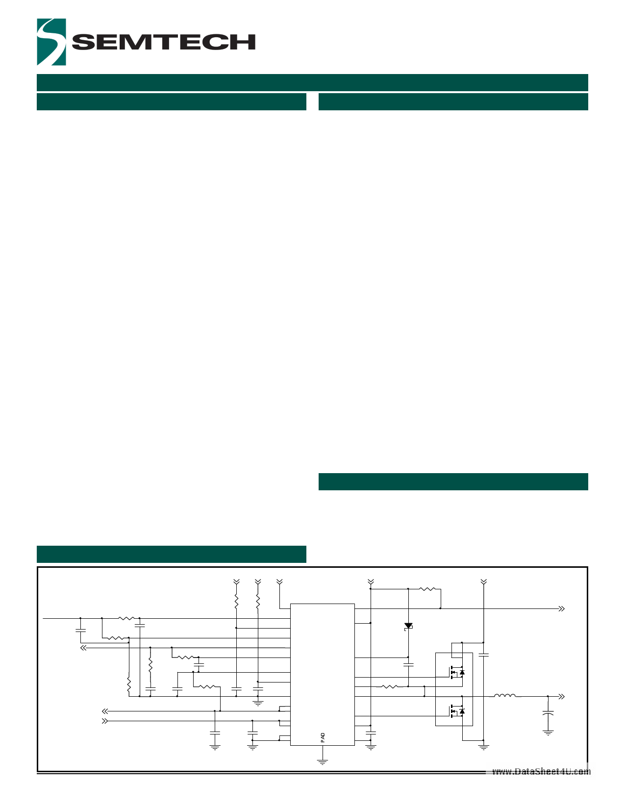
Typical Application Circuit
SC486
Complete DDR1/2/3
Memory Power Supply
Features
DDR1, DDR2 and DDR3 compatible
Constant on-time controller for fast dynamic
response on VDDQ
Programmable VDDQ range - 1.5V to 3V
1% Internal Reference (2% System Accuracy)
Resistor programmable on time for VDDQ
VCCA/VDDP range = 4.5V to 5.5V
VBAT range = 2.5V to 25V
VDDQ DC current sense using low-side RDS(ON)
sensing or external RSENSE in series with low-side
FET
Cycle-by-cycle current limit for VDDQ
Digital soft-start for VDDQ
Combined EN and PSAVE pin for VDDQ
Over-voltage/under-voltage fault protection for
both outputs and PGD output (VDDQ only)
Separate VCCA and VDDP supplies
VTT/REF range = 0.75V – 1.5V
VTT source/sink 3A peak
Internal resistor divider for VTT/REF
VTT is high impedance in S3
VDDQ, VTT and REF are actively discharged in
S4/S5
24-pin MLPQ (4 x 4mm) Lead-free package, fully
WEEE and RoHS compliant
Applications
Notebook computers
CPU I/O supplies
Handheld terminals and PDAs
LCD monitors
Network power supplies
VBAT 5VSUS 5VRUN
VDDQ
R4 10R
C1
no-pop
R5
C2
1uF
REF
R6
10R
R9
C6
1uF
VTT
VDDQ
R7 10R
C3
no-pop
R8 0R
C7
no-pop
C11
20uF
R1 R2
10R
C8 C9
1nF 1uF
C12
1uF
U1
11 VTTEN
3 VDDQS
2 TON
6 FB
8 REF
9 COMP
10 VTTS
5 VCCA
4 VSSA
14
15
VTT
VTT
12
13
VTTIN
VTTIN
16
17
PGND2
PGND2
5VSUS
SC486
PGD 7
EN/PSV 1
BST 24
DH
ILIM
LX
23
21
22
R10
DL
VDDP
19
20
PGND1 18
C13
1uF
R3 470k
VBAT
D1
C4
0.1uF
4
3
8
56
C5
10uF
L1
7
2
Q1
1
PGOOD
VDDQ
+ C10
Revision: September 13, 2006
1
www.semtech.com
1 page 
SC486
POWER MANAGEMENT
Electrical Characteristics (Cont.)
Test Conditions: VBAT = 15V, VCCA = VDDP = VTTEN = EN/PSV = 5V, VDDQ = VTTIN = 1.8V, RTON = 1MΩ
Parameter
Conditions
25°C
-40°C to 125°C Units
Min Typ Max Min Max
Gate Drives (Cont.)
DL Pull-Up Resistance
DL high
2
4Ω
DL Source Current
www.DataSDheHet4PUu.lcl-oDmown Resistance
VDL = 2.5V
DH low, BST - LX = 5V
1.3
2
A
4Ω
DH Pull-Up Resistance(8)
DH high, BST - LX = 5V
2
4Ω
DH Sink/Source Current
VTT Pull-Up Resistance
VDH = 2.5V
VTTS < REF
1.3
0.25
A
0.45 Ω
VTT Pull-Down Resistance
VTTS > REF
0.25
0.45 Ω
VTT Peak Sink/Source Current (9)
3.6 2.0
A
Notes:
(1) The output voltage will have a DC regulation level higher than the error-comparator threshold by 50% of the
ripple voltage.
(2) Using a current sense resistor, this measurement relates to PGND1 minus the voltage of the source on the
low-side MOSFET.
(3) clks = switching cycles, consisting of one high side and one low side gate pulse.
(4) Guaranteed by design.
(5) Thermal shutdown latches both outputs (VTT and VDDQ) off, requiring VCCA or EN/PSV cycling to reset.
(6) VTT soft start ramp rate is 6mV/µs typical unless VDDQ/2 ramp rate is slower. If this is true, VTT soft start
ramps at 6mV/µs (typ.) until it reaches VDDQ/2, and then tracks it.
(7) See Shoot-Through Delay Timing Diagram below.
(8) Semtech’s SmartDriver™ FET drive first pulls DH high with a pull-up resistance of 10Ω (typ.) until LX = 1.5V
(typ.). At this point, an additional pull-up device is activated, reducing the resistance to 2Ω (typ.). This negates the
need for an external gate or boost resistor.
(9) Provided operation below TJ(MAX) is maintained.
(10) This device is ESD sensitive. Use of standard ESD handling precautions is required.
Shoot-Through Delay Timing Diagram
LX
DH
DL
tplhDL
DL
tplhDH
2006 Semtech Corp.
5
www.semtech.com
5 Page 
SC486
POWER MANAGEMENT
EN/PSV: Enable, PSAVE and Soft Discharge (Cont.)
If the EN/PSV pin is pulled low, all three outputs will be
shut down and discharged using switches with a nominal
resistance of 22 Ohms, regardless of the state of the
VTTEN pin. This will ensure that the outputs will be in a
defined state next time they are enabled and also
ensure, since this is a soft discharge, that there are no
dangerous negative voltage excursions to be concerned
about. In order for the soft discharge circuitry to
function correctly, the chip supply must be present.
www.DataVShTeTeEt4NU.com
The VTTEN pin is used to enable the VTT regulator only.
Pulling it high enables the regulator as long as VDDQ/
REF are present. Pulling VTTEN low while EN/PSV is
floating or high will turn off the VTT regulator and leave it
in a high-impedance state for S3 mode (VDDQ and REF
present, VTT high-Z).
VDDQ Output Voltage Selection and Output Sense
The output voltage is set by the feedback resistors R5 &
R9 of Figure 2 below. The internal reference is 1.5V, so
the voltage at the feedback pin will match the 1.5V
reference. Therefore the output can be set to a
minimum of 1.5V. The equation for setting the output
voltage is:
VOUT
=
1 +
R5
R8
• 1.5
VDDQS is used to sense the output voltages for the on-
time one-shot, tON, and also to generate REF, which is 1/
2 of VDDQ. An RC filter consisting of 10Ω and 1µF from
VDDQ to VSSA is required (R4 and C2 in Figure 2) to filter
switching frequency ripple.
VDDQ Current Limit Circuit
Current limiting of the SC486 can be accomplished in
two ways. The on-state resistance of the low-side
MOSFETs can be used as the current sensing element or
sense resistors in series with the low-side sources can
be used if greater accuracy is desired. RDS(ON)
sensing is more efficient and less expensive. In both
cases, the RILIM resistors between the ILIM pin and LX pin
set the over current threshold. This resistor RILIM is
connected to a 10µA current source within the SC486
which is turned on when the low side MOSFET turns on.
When the voltage drop across the sense resistor or low
side MOSFET equals the voltage across the RILIM
resistor, positive current limit will activate. The high side
MOSFET will not be turned on until the voltage drop across
the sense element (resistor or MOSFET) falls below the
voltage across the RILIM resistor. In an extreme over-
current situation, the top MOSFET will never turn back
on and eventually the part will latch off due to output
undervoltage (see Output Undervoltage Protection).
The current sensing circuit actually regulates the
inductor valley current (see Figure 3). This means that if
the current limit is set to 10A, the peak current through
the inductor would be 10A plus the peak ripple current,
and the average current through the inductor would be
10A plus 1/2 the peak-to-peak ripple current. The
equations for setting the valley current and calculating
the average current through the inductor are shown
overleaf.
VBAT 5VSUS 5VRUN
VDDQ
C1
no-pop
R4 10R
R5
C2
1uF
REF
R6
10R
R9
C6
1uF
VTT
VDDQ
R7 10R
C3
no-pop
R8 0R
C7
no-pop
C11
20uF
R1 R2
10R
C8 C9
1nF 1uF
C12
1uF
U1
11 VTTEN
3 VDDQS
2 TON
6 FB
8 REF
9 COMP
10 VTTS
5 VCCA
4 VSSA
14
15
VTT
VTT
12
13
VTTIN
VTTIN
16
17
PGND2
PGND2
5VSUS
SC486
PGD 7
EN/PSV 1
BST 24
DH
ILIM
LX
23
21
22
R10
DL
VDDP
19
20
PGND1 18
C13
1uF
R3 470k
VBAT
D1
C4
0.1uF
4
3
8
56
C5
10uF
L1
7
2
Q1
1
PGOOD
VDDQ
+ C10
2006 Semtech Corp.
Figure 2
11
www.semtech.com
11 Page | ||
| Páginas | Total 26 Páginas | |
| PDF Descargar | [ Datasheet SC486.PDF ] | |
Hoja de datos destacado
| Número de pieza | Descripción | Fabricantes |
| SC480 | Complete DDR1/2/3 Memory Power Supply | Semtech Corporation |
| SC4806 | Multiple Function Double Ended PWM Controller | Semtech Corporation |
| SC4808A | High Performance Dual Ended PWM Controller | Semtech Corporation |
| SC4808B | High Performance Dual Ended PWM Controller | Semtech Corporation |
| Número de pieza | Descripción | Fabricantes |
| SLA6805M | High Voltage 3 phase Motor Driver IC. |
Sanken |
| SDC1742 | 12- and 14-Bit Hybrid Synchro / Resolver-to-Digital Converters. |
Analog Devices |
|
DataSheet.es es una pagina web que funciona como un repositorio de manuales o hoja de datos de muchos de los productos más populares, |
| DataSheet.es | 2020 | Privacy Policy | Contacto | Buscar |