|
|
|
PDF SC4605 Data sheet ( Hoja de datos )
| Número de pieza | SC4605 | |
| Descripción | Step Down Controller | |
| Fabricantes | Semtech Corporation | |
| Logotipo | ||
Hay una vista previa y un enlace de descarga de SC4605 (archivo pdf) en la parte inferior de esta página. Total 19 Páginas | ||
|
No Preview Available !
POWER MANAGEMENT
Description
SC4605
Low Input, High Efficiency
Synchronous, Step Down Controller
Features
The SC4605 is a voltage mode step down (buck) regula-
tor controller that provides accurate high efficiency power
conversion from a input supply range of 2.8V to 5.5V. A
high level of integration reduces external component
count, and makes it suitable for low voltage applications
where cost, size and efficiency are critical.
The SC4605 drives external N-channel MOSFETs with 1A
www.DatapSeheaekt4Uc.ucormrent. A non-overlap protection is provided for
the gate drive signals to prevent shoot through of the
MOSFET pair. The voltage drop across the high side
MOSFET during its conduction is sensed for lossless short
circuit current limiting.
BICMOS voltage mode PWM controller
2.8V to 5.5V Input voltage range
Output voltages as low as 0.8V
+/-1% Reference accuracy
Sleep mode (Icc = 10µA typ)
Lossless adjustable short circuit current limiting
Combination pulse by pulse & hiccup mode
current limit
High efficiency synchronous switching
0% to 97% Duty cycle range
1A Peak current driver
10-Pin MSOP package
The quiescent supply current in sleep mode is typically
lower than 10µA. A 1.8ms soft start is internally provided
to prevent output voltage overshoot during start-up.
The SC4605 is an ideal choice for 3.3V, 5V or other low
input supply systems. It’s available in 10 pin MSOP pack-
age.
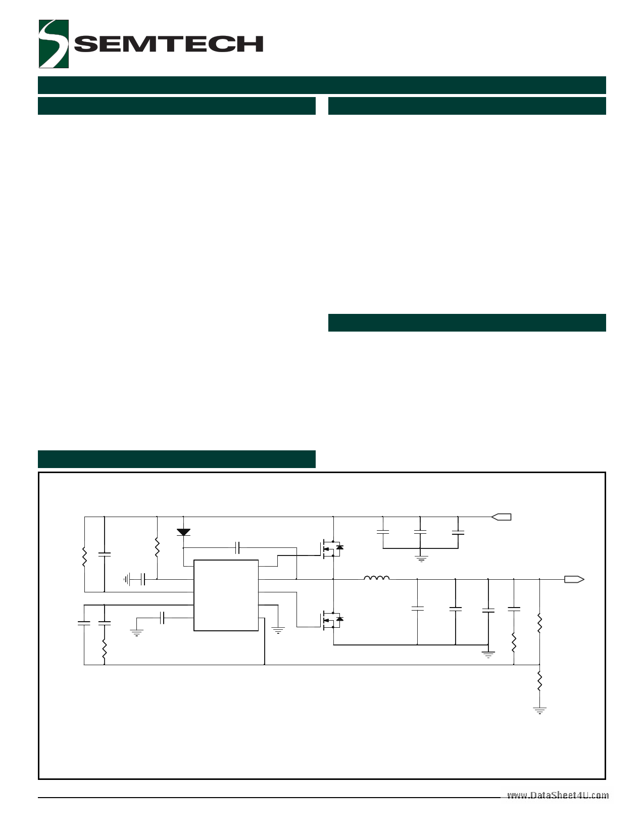
Typical Application Circuit
Applications
Distributed power architecture
Servers/workstations
Local microprocessor core power supplies
DSP and I/O power supplies
Battery powered applications
Telecommunications equipment
Data processing applications
R3 C14
0. 1u
C1
180p
C2 2.2n
R1
14.3k
R 13
1
C3
4. 7u
C 20
470pF
D2 1u
C 71
U1
1 BST
2 VCC
3 ISET
4 COMP
5 FFSS/ESTYNC
DRVH
PHASE
DRVL
GND
VSENSE
10
9
8
7
6
SC4605
Vin = 2.8V - 5.5V
C10 C11 C12
220u 22u 22u
M1
L1 Vout = 1.5V (as low as 0.8V * ) / 12A
1. 8u
C6 C5 C4 C9
M2
330u
22u 22u 4.7n R7
10k
R8
200
R9
11.5k
* External components can be modified to provide a Vout as low as 0.8V.
Revision: October 14, 2004
1
www.semtech.com
1 page 
POWER MANAGEMENT
Block Diagram
www.DataSheet4U.com
SC4605
Marking Information
yyww = Datecode (Example: 0012)
xxxx = Semtech Lot # (Example: E901
xxxx
01-1)
2004 Semtech Corp.
5
www.semtech.com
5 Page 
SC4605
POWER MANAGEMENT
Applications Information (Cont.)
Layout Guideline
The design guidelines for the SC4605 applications are
as following:
1.
Set the loop gain crossover corner frequency
given switching corner frequency ωS =2πfs,
ωC
for
2. Place an integrator at the origin to increase DC and
low frequency gains,
3.
SωeOletoctdaωmZ1patnhde
pωeZa2ksiuncghatnhdatthteheloyoapregapilnacheads
near
a
www.DataSheet4U.co-m20dB/dec rate to go across the 0dB line for
obtaining a wide bandwidth,
4.
Cancel the zero
pole ωP1 ( ωP1 =
from
ωESR
=C41’s/(ERSCRC4b))y,
a
compensator
5. Place a high frequency compensator pole
ωp2 ( ωp2 = πfs) to get the maximum attenuation of
the switching
ripple and high frequency noise with the adequate
phase lag at ωC.
The compensated loop gain will be as given in Figure 4:
T
ωZ1 ωo
Loop gain T(s)
ωZ2 -20dB/dec
Gvd
ωc
0dB
ωp1
ω p2
Power stage GVD(s)
-40dB/dec
ω ESR
In order to achieve optimal electrical, thermal and noise
performance for high frequency converters, special at-
tention must be paid to the PCB layouts. The goal of lay-
out optimization is to identify the high di/dt loops and
minimize them. The following guideline should be used to
ensure proper functions of the converters.
1. A ground plane is recommended to minimize noises
and copper losses, and maximize heat dissipation.
2. Start the PCB layout by placing the power compo-
nents first. Arrange the power circuit to achieve a
clean power flow route. Put all the connections on
one side of the PCB with wide copper filled areas if
possible.
3. The Vcc bypass capacitor should be placed next to
the Vcc and GND pins.
4. The trace connecting the feedback resistors to the
output should be short, direct and far away from the
noise sources such as switching node and switching
components.
5. Minimize the traces between DRVH/DRVL and the
gates of the MOSFETs to reduce their impedance to
drive the MOSFETs.
6. Minimize the loop including input capacitors, top/bot-
tom MOSFETs. This loop passes high di/dt current.
Make sure the trace width is wide enough to reduce
copper losses in this loop.
7. ISET and PHASE connections to the top MOSFET for
current sensing must use Kelvin connections.
8. Maximize the trace width of the loop connecting the
inductor, bottom MOSFET and the output capacitors.
9. Connect the ground of the feedback divider and the
compensation components directly to the GND pin
of the SC4605 by using a separate ground trace.
Then connect this pin to the ground of the output
capacitor as close as possible.
Figure 4. Asymptotic diagrams of power stage and its
loop gain
2004 Semtech Corp.
11
www.semtech.com
11 Page | ||
| Páginas | Total 19 Páginas | |
| PDF Descargar | [ Datasheet SC4605.PDF ] | |
Hoja de datos destacado
| Número de pieza | Descripción | Fabricantes |
| SC4601 | Step Down Controller | Semtech Corporation |
| SC4602A | Step Down Controller | Semtech Corporation |
| SC4602B | Step Down Controller | Semtech Corporation |
| SC4603 | High Efficiency Synchronous Buck | Semtech Corporation |
| Número de pieza | Descripción | Fabricantes |
| SLA6805M | High Voltage 3 phase Motor Driver IC. |
Sanken |
| SDC1742 | 12- and 14-Bit Hybrid Synchro / Resolver-to-Digital Converters. |
Analog Devices |
|
DataSheet.es es una pagina web que funciona como un repositorio de manuales o hoja de datos de muchos de los productos más populares, |
| DataSheet.es | 2020 | Privacy Policy | Contacto | Buscar |