|
|
|
PDF ADT7467 Data sheet ( Hoja de datos )
| Número de pieza | ADT7467 | |
| Descripción | dBCool Remote Thermal Monitor and Fan Controller | |
| Fabricantes | Analog Devices | |
| Logotipo | ||
Hay una vista previa y un enlace de descarga de ADT7467 (archivo pdf) en la parte inferior de esta página. Total 30 Páginas | ||
|
No Preview Available !
FEATURES
Controls and monitors up to 4 fans
High and low frequency fan drive signal
1 on-chip and 2 remote temperature sensors
Series resistance cancellation on the remote channel
Extended temperature measurement range, up to 191°C
Dynamic TMIN control mode intelligently optimizes
system acoustics
Automatic fan speed control mode manages system cooling
based on measured temperature
Enhanced acoustic mode dramatically reduces user perception
of changing fan speeds
Thermal protection feature via THERM output
Monitors performance impact of Intel® Pentium® 4 processor
Thermal control circuit via THERM input
2-wire, 3-wire, and 4-wire fan speed measurement
Limit comparison of all monitored values
Meets SMBus 2.0 electrical specifications
(fully SMBus 1.1 compliant)
dBCool® Remote Thermal
Monitor and Fan Controller
ADT7467
GENERAL DESCRIPTION
The ADT7467 dBCool controller is a thermal monitor and
multiple PWM fan controller for noise-sensitive or power-
sensitive applications requiring active system cooling. The
ADT7467 can drive a fan using either a low or high frequency
drive signal, monitor the temperature of up to two remote
sensor diodes plus its own internal temperature, and measure
and control the speed of up to four fans so that they operate at
the lowest possible speed for minimum acoustic noise.
The automatic fan speed control loop optimizes fan speed for a
given temperature. A unique dynamic TMIN control mode
enables the system thermals/acoustics to be intelligently
managed. The effectiveness of the system’s thermal solution can
be monitored using the THERM input. The ADT7467 also
provides critical thermal protection to the system using the
bidirectional THERM pin as an output to prevent system or
component overheating.
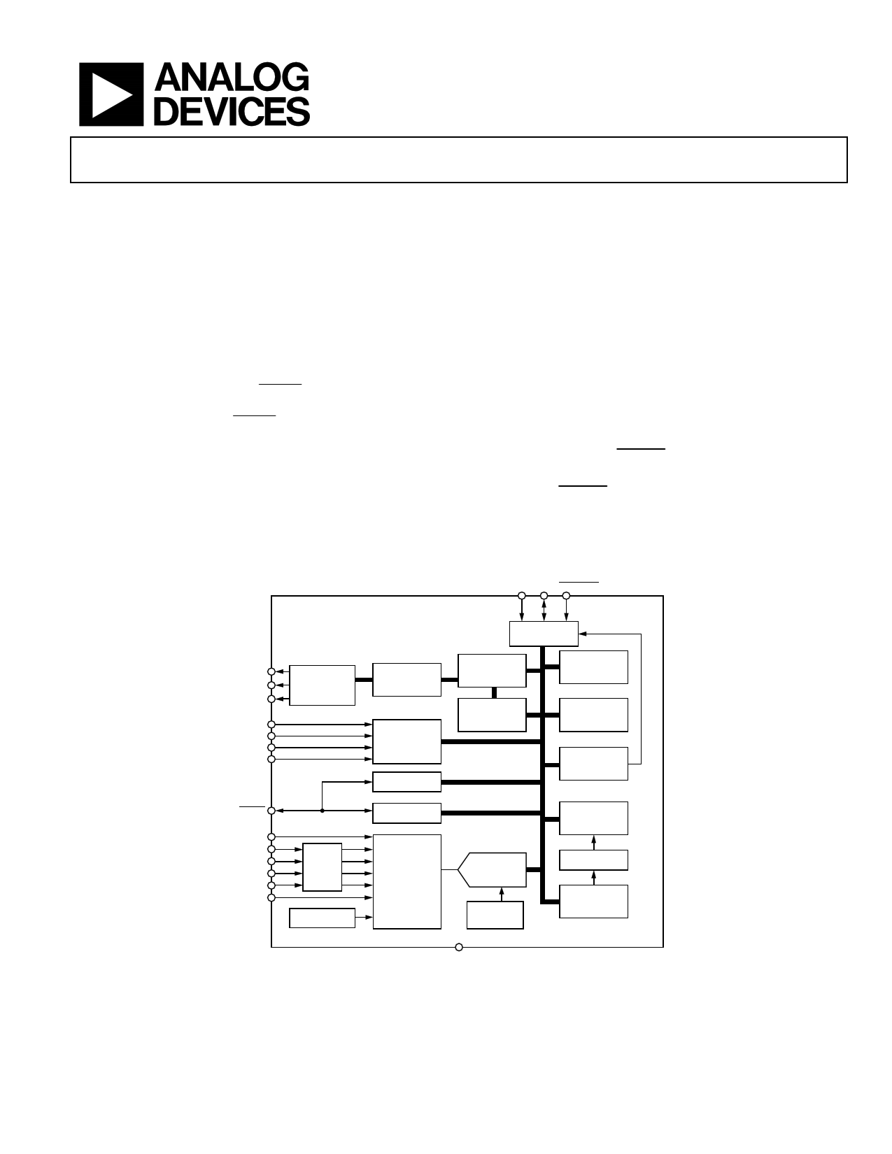
FUNCTIONAL BLOCK DIAGRAM
SCL SDA SMBALERT
PWM1
PWM2
PWM3
TACH1
TACH2
TACH3
TACH4
THERM
VCC
D1+
D1–
D2+
D2–
VCCP
PWM REGISTERS
AND
CONTROLLERS
HF & LF
VCC TO ADT7467
SRC
BAND GAP
TEMP SENSOR
ACOUSTIC
ENHANCEMENT
CONTROL
FAN SPEED
COUNTER
PERFORMANCE
MONITORING
SERIAL BUS
INTERFACE
AUTOMATIC
FAN SPEED
CONTROL
ADDRESS
POINTER
REGISTER
DYNAMIC
TMIN
CONTROL
PWM
CONFIGURATION
REGISTERS
INTERRUPT
MASKING
THERMAL
PROTECTION
ADT7467
INPUT
SIGNAL
CONDITIONING
AND
ANALOG
MULTIPLEXER
10-BIT
ADC
BAND GAP
REFERENCE
GND
INTERRUPT
STATUS
REGISTERS
LIMIT
COMPARATORS
VALUE AND
LIMIT
REGISTERS
Figure 1.
Rev. A
Information furnished by Analog Devices is believed to be accurate and reliable.
However, no responsibility is assumed by Analog Devices for its use, nor for any
infringements of patents or other rights of third parties that may result from its use.
Specifications subject to change without notice. No license is granted by implication
or otherwise under any patent or patent rights of Analog Devices. Trademarks and
registered trademarks are the property of their respective owners.
One Technology Way, P.O. Box 9106, Norwood, MA 02062-9106, U.S.A.
Tel: 781.329.4700
www.analog.com
Fax: 781.461.3113 © 2005 Analog Devices, Inc. All rights reserved.
1 page 
ABSOLUTE MAXIMUM RATINGS
Table 2.
Parameter
Positive Supply Voltage (VCC)
Voltage on Any Input or Output Pin
Input Current at Any Pin
Package Input Current
Maximum Junction Temperature (TJMAX)
Storage Temperature Range
Lead Temperature, Soldering
IR Reflow Peak Temperature
For Pb-free models
Lead Temperature (Soldering 10 sec)
ESD Rating
Rating
5.5 V
−0.3 V to +6.5 V
±5 mA
±20 mA
150°C
−65°C to +150°C
220°C
260°C
300°C
1000 V
ADT7467
Stresses above those listed under Absolute Maximum Ratings
may cause permanent damage to the device. This is a stress
rating only; functional operation of the device at these or any
other conditions above those indicated in the operational
section of this specification is not implied. Exposure to absolute
maximum rating conditions for extended periods may affect
device reliability.
THERMAL CHARACTERISTICS
16-lead QSOP package:
θJA = 150°C/W
θJC = 39°C/W
ESD CAUTION
ESD (electrostatic discharge) sensitive device. Electrostatic charges as high as 4000 V readily accumulate on
the human body and test equipment and can discharge without detection. Although this product features
proprietary ESD protection circuitry, permanent damage may occur on devices subjected to high energy
electrostatic discharges. Therefore, proper ESD precautions are recommended to avoid performance
degradation or loss of functionality.
Rev. A| Page 5 of 80
5 Page 
SERIAL BUS INTERFACE
On PCs and servers, control of the ADT7467 is carried out
using the serial system management bus (SMBus). The
ADT7467 is connected to this bus as a slave device under the
control of a master controller, which is usually (but not
necessarily) the ICH.
The ADT7467 has a fixed 7-bit serial bus address of 0101110 or
0x2E. The read/write bit must be added to get the 8-bit address
(01011100 or 0x5C). Data is sent over the serial bus in
sequences of nine clock pulses: eight bits of data followed by an
acknowledge bit from the slave device. Transitions on the data
line must occur during the low period of the clock signal and
remain stable during the high period, because a low-to-high
transition might be interpreted as a stop signal when the clock
is high. The number of data bytes that can be transmitted over
the serial bus in a single read or write operation is only limited
by what the master and slave devices can handle.
When all data bytes have been read or written, stop conditions
are established. In write mode, the master pulls the data line
high during the 10th clock pulse to assert a stop condition. In
read mode, the master device overrides the acknowledge bit by
pulling the data line high during the low period before the
ninth clock pulse. This is known as a no acknowledge. The
master then takes the data line low during the low period before
the 10th clock pulse, and then high during the 10th clock pulse
to assert a stop condition.
Any number of bytes of data can be transferred over the serial
bus in one operation. It is not possible to mix a read and a write
in one operation, however, because the type of operation is
determined at the beginning and cannot subsequently be
changed without starting a new operation.
In the ADT7467, write operations contain either one or two
bytes, and read operations contain one byte. To write data to a
device data register or read data from it, the address pointer
register must first be set. The first byte of a write operation
always contains an address, which is stored in the address
pointer register, and the second byte, if there is a second byte, is
written to the register selected by the address pointer register.
ADT7467
This write operation is illustrated in Figure 16. The device
address is sent over the bus, and then R/W is set to 0. This is
followed by two data bytes. The first data byte is the address of
the internal data register, and the second data byte is the data
written to that internal data register.
When reading data from a register, there are two possibilities:
• If the address pointer register value of the ADT7467 is
unknown or not the desired value, it must be set to the
correct value before data can be read from the desired data
register. This is achieved by writing a data byte containing
the register address to the ADT7467. This is shown in
Figure 17. A read operation is then performed consisting of
the serial bus address and the R/W bit set to 1, followed by
the data byte read from the data register. This is shown in
Figure 18.
• If the address pointer register is known to be at the desired
address, data can be read from the corresponding data
register without first writing to the address pointer register,
as shown in Figure 18.
If the address pointer register is already at the correct value, it is
possible to read a data byte from the data register without first
writing to the address pointer register. However, it is not
possible to write data to a register without writing to the
address pointer register, because the first data byte of a write is
always written to the address pointer register.
In addition to supporting the send byte and receive byte
protocols, the ADT7467 also supports the read byte protocol.
(See Intel’s System Management Bus Specifications Rev. 2 for
more information.)
If several read or write operations must be performed in
succession, the master can send a repeat start condition instead
of a stop condition to begin a new operation.
Rev. A| Page 11 of 80
11 Page | ||
| Páginas | Total 30 Páginas | |
| PDF Descargar | [ Datasheet ADT7467.PDF ] | |
Hoja de datos destacado
| Número de pieza | Descripción | Fabricantes |
| ADT7460 | dB COOL Remote Thermal Controller and Fan Controller | Analog Devices |
| ADT7461 | Temperature Monitor | Analog Devices |
| ADT7461 | Temperature Monitor | ON Semiconductor |
| ADT7461A | Temperature Monitor | ON Semiconductor |
| Número de pieza | Descripción | Fabricantes |
| SLA6805M | High Voltage 3 phase Motor Driver IC. |
Sanken |
| SDC1742 | 12- and 14-Bit Hybrid Synchro / Resolver-to-Digital Converters. |
Analog Devices |
|
DataSheet.es es una pagina web que funciona como un repositorio de manuales o hoja de datos de muchos de los productos más populares, |
| DataSheet.es | 2020 | Privacy Policy | Contacto | Buscar |