|
|
|
PDF ISL5416 Data sheet ( Hoja de datos )
| Número de pieza | ISL5416 | |
| Descripción | Four-Channel Wideband Programmable DownConverter | |
| Fabricantes | Intersil Corporation | |
| Logotipo | ||
Hay una vista previa y un enlace de descarga de ISL5416 (archivo pdf) en la parte inferior de esta página. Total 30 Páginas | ||
|
No Preview Available !
®
Data Sheet
February 2003
ISL5416
FN6006.2
Four-Channel Wideband Programmable
DownConverter
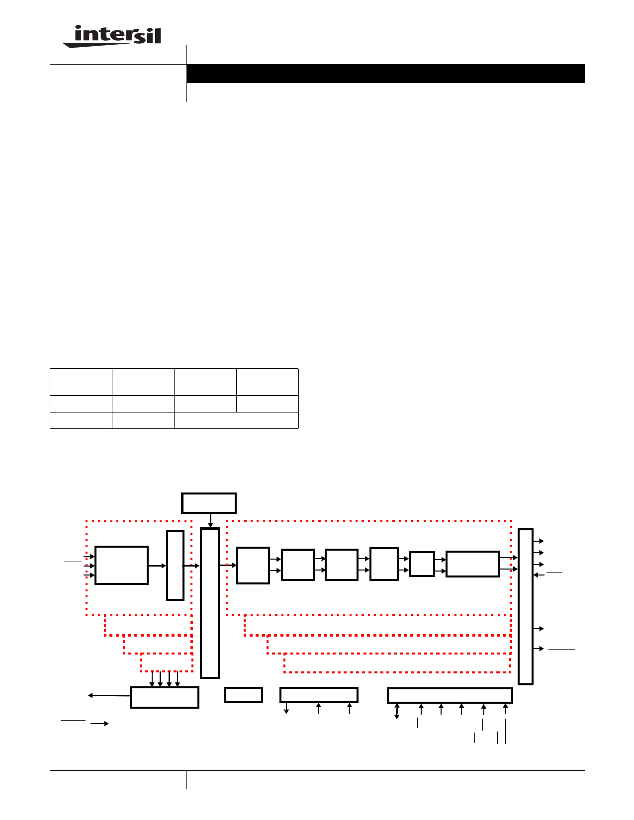
The ISL5416 Four-Channel Wideband Programmable Digital
DownConverter (WPDC) is designed for high dynamic range
applications such as cellular basestations where the
processing of multiple channels is required in a small
physical space. The WPDC combines four channels in a
single package, each including: an NCO, a digital mixer,
digital filters, an AGC and a resampling filter.
All channels are independently programmable and may be
updated in real time. Each of the four channels can select
any of the four digital input buses. Each of the tuners can
process a W-CDMA channel. Channels may be cascaded or
polyphased for increased bandwidth. Selectable outputs
include I samples, Q samples, and AGC gain. Outputs from
the part are available over the parallel, serial or uP
interfaces.
Ordering Information
PART
NUMBER
TEMP
RANGE (oC)
ISL5416KI
-40 to 85
ISL5416EVAL1
25
PACKAGE
PKG. NO
256 BGA
V256.17x17
EVALUATION KIT
Features
• Up to 95MSPS Input
• Four Parallel 16-bit Fixed or 17-bit Floating Point Inputs
• Programmable RF Attenuator/VGA Control
• 32-Bit Programmable Carrier NCO with > 110dB SFDR
• 20-bit Internal Data Path
• Filter Functions
- Multi-Stage Cascaded-Integrator-Comb (CIC) Filter
- Two programmable FIR Filters (first up to 32-taps,
second up to 64-taps)
- Half Band Interpolation Filter
- Resampling FIR Filter
• Overall decimation from 1 to >4096
• Digital AGC with up to 96dB of Gain Range
• Up to Four Independent 16-bit Parallel Outputs
• Serial Output Option
• 16-bit Parallel µP Interface
• 1.8V core, 3.3V I/O Operation
• Evaluation Board and Configuration Software available
Applications
• Basestation Receivers: GSM/EDGE, CDMA2000, UMTS.
Block Diagram
TEST
REGISTER
OUTPUT
AIN(16:0)
ENIA
CLKA
INPUT
SELECT
CLOCK &
FORMAT
NCO I
MIXER
CIC Q
I
FIR1
FILTER
Q
I
FIR2
FILTER
Q
I
AGC
Q
I
IHBF
Q
RESAMPLER
I
Q
AOUT(15:8)
AOUT(7:0)
FSYNCA
OEA
INPUT A
INPUT B
INPUT C
INPUT D
EOUT(15:0)
RESET
RF ATTENUATOR
VGA CONTROL
JTAG
SYNCHRONIZATION
SYNCO SYNCIN1 SYNCIN2
CHANNEL O
CHANNEL 1
CHANNEL 2
CHANNEL 3
µP INTERFACE
CLKO1
CLKO2
/INTRPT
1
CAUTION: These devices are sensitive to electrostatic discharge; follow proper IC Handling Procedures.
1-888-INTERSIL or 321-724-7143 | Intersil (and design) is a registered trademark of Intersil Americas Inc.
Copyright © Intersil Americas Inc. 2003. All Rights Reserved
All other trademarks mentioned are the property of their respective owners.
1 page 
ISL5416
Pin Descriptions (Continued)
NAME
INTERNAL
TYPE PULL-UP/DOWN
DESCRIPTION
JTAG
TDO
O
Test data out
TDI
I
PULL UP
Test data in.
TMS
I
PULL UP
Test mode select.
TCLK
I PULL DOWN Test clock.
TRST
I
PULL UP
Test reset. Active low. If JTAG not used, tie this pin low. If there is a trace connected to the pin and
there is enough board noise, the JTAG port might get into an unexpected state and stop
communications with the part
OUTPUTS
Aout(15:0)
O
Parallel Data Output bus A. A 16-bit parallel data output which can be programmed to consist of I, Q,
AGC. Data from Channels 0, 1, 2 and 3 can be multiplexed into a common parallel output data bus.
Information can be sequenced in a programmable order. Can be ones complemented. Can be
divided into two 8-bit busses. See Data Output Formatter Section and Microprocessor Interface
Section. See Table 24.
Bout(15:0)
O
Parallel Data Output bus B. A 16-bit parallel data output which can be programmed to consist of I, Q,
AGC. Data from Channels 0, 1, 2 and 3 can be multiplexed into a common parallel output data bus.
Information can be sequenced in a programmable order. Can be ones complemented. Can be
divided into two 8-bit busses. See Data Output Formatter Section and Microprocessor Interface
Section.
Cout(15:0)
O
Parallel Data Output bus C. A 16-bit parallel data output which can be programmed to consist of I, Q,
AGC. Data from Channels 0, 1, 2 and 3 can be multiplexed into a common parallel output data bus.
Information can be sequenced in a programmable order. Can be ones complemented. Can be
divided into two 8-bit busses. See Data Output Formatter Section and Microprocessor Interface
Section.
Dout(15:0)
O
Parallel Data Output bus D. A 16-bit parallel data output which can be programmed to consist of I, Q,
AGC. Data from Channels 0, 1, 2 and 3 can be multiplexed into a common parallel output data bus.
Information can be sequenced in a programmable order. Can be ones complemented. Can be
divided into two 8-bit busses. See Data Output Formatter Section and Microprocessor Interface
Section.
Below is the table of the serial output bits allocation for DOUT.
Eout(15:0)
CLKO1
O
O
CLKO2/
INTRPT
O
SERIAL OUTPUT BITS ALLOCATION
SER. OUTPUT A SER. OUTPUT B SER. OUTPUT C SER. OUTPUT D
SCLKX *
DOUT0
DOUT4
DOUT8
DOUT12
SSYNCX *
DOUT1
DOUT5
DOUT9
DOUT13
SD1X *
DOUT2
DOUT6
DOUT10
DOUT14
SD2X *
DOUT3
DOUT7
DOUT11
DOUT15
* X denotes A, B, C, D as appropriate
A 16-bit parallel VGA/Attenuator control output. Partitionable into separate 4 or 8-bit busses.
Output Clock 1. Can be programmed to be at CLKC/N for N = 1 to 16. The polarity of CLKO1 is
programmable.
Available ONLY on Rev B (final) version of the part. Provides a complementary output or a second
clock to simplify board routing. Polarity is programmable. It can also be programmed as an interrupt
from one or more channels for a sequenced read (FIFO-like) mode. See register GWA = 0000h, bit
13.
5
5 Page 
ISL5416
NCO / Mixer
After the input select/format section, the samples are
multiplied by quadrature sine wave samples from the carrier
NCO. The NCO has a 32-bit frequency control, providing
sub-hertz resolution at the maximum clock rate. The
quadrature sinusoids have exceptional purity. The purity of
the NCO should not be the determining factor for the
receiver dynamic range performance (A typical spectrum
plot is shown in Figure 20). The phase quantization to the
sine/cosine generator is 24 bits and the amplitude
quantization is 19 bits.
The carrier NCO center frequency is loaded via the uP bus. The
center frequency control is double buffered -- the input is loaded
into a holding register via the uP interface. The data is then
transferred from the holding register to the active register by a
write to a special address or by a SYNCInX signal, if enabled in
IWA = *000h. To synchronize multiple channels, the carrier
NCO phase accumulator feedback can be zeroed on loading to
restart all of the NCOs at the same phase (see IWA = *005h).
The phase of the NCO can be offset by programming IWA =
*003h. The phase offset is not double buffered.
ENA
ENB
ENC
END
ENµP
EXPA
EXPB
EXPC
EXPD
EXPµP
AMANT
BMANT
CMANT
DMANT
µPMANT
(TEST INPUT)
RR
EE
GG
MAX EXP
C
RR L
EE I
GG P
RRR
EEE
GGG
RRR
EEE
GGG
R R 0...-15
EE
GG
0...-23
RRR
EEE
GGG
0...-18
REG
REG
SIN/COS
GEN
REG
0...-23
R
DECIMATION E
COUNTER G
BASE
SHIFT
VALUE
(from uP)
0...-23
R
E
G
34b
44b
53b
62b
69b
RRR
EEE
GGG
0...-29
0...-23
FIR R R R
FILTER
(COMB)
E
G
E
G
E
G
R
E
G
ENCOF
COF
COFSYNC
SERIAL
FREQ
OFFSET
REG
REG
REG
REG
CENTER PHASE
FREQ
OFFSET
CIC ORDER
1
2
3
4
5
FIR COEFFICIENTS
1 -1
1 -2
1
1 -3 3 -1
1 -4 6
-4 1
1 -5 10 -10 5 -1
NOTE:
BUS NUMBERING SUCH AS 0...-23 INDICATES BIT WEIGHTS
SUCH AS 20 ... 2-23
FIGURE 3. NCO, MIXER AND CIC BLOCK DIAGRAM
11
11 Page | ||
| Páginas | Total 30 Páginas | |
| PDF Descargar | [ Datasheet ISL5416.PDF ] | |
Hoja de datos destacado
| Número de pieza | Descripción | Fabricantes |
| ISL54100 | TMDS Regenerators | Intersil |
| ISL54100A | TMDS Regenerators | Intersil |
| ISL54101 | TMDS Regenerators | Intersil |
| ISL54101A | TMDS Regenerators | Intersil |
| Número de pieza | Descripción | Fabricantes |
| SLA6805M | High Voltage 3 phase Motor Driver IC. |
Sanken |
| SDC1742 | 12- and 14-Bit Hybrid Synchro / Resolver-to-Digital Converters. |
Analog Devices |
|
DataSheet.es es una pagina web que funciona como un repositorio de manuales o hoja de datos de muchos de los productos más populares, |
| DataSheet.es | 2020 | Privacy Policy | Contacto | Buscar |