|
|
|
PDF AD585 Data sheet ( Hoja de datos )
| Número de pieza | AD585 | |
| Descripción | High Speed/ Precision Sample-and-Hold Amplifier | |
| Fabricantes | Analog Devices | |
| Logotipo | ||
Hay una vista previa y un enlace de descarga de AD585 (archivo pdf) en la parte inferior de esta página. Total 6 Páginas | ||
|
No Preview Available !
a
High Speed, Precision
Sample-and-Hold Amplifier
AD585
FEATURES
3.0 s Acquisition Time to ؎0.01% max
Low Droop Rate: 1.0 mV/ms max
Sample/Hold Offset Step: 3 mV max
Aperture Jitter: 0.5 ns
Extended Temperature Range: –55؇C to +125؇C
Internal Hold Capacitor
Internal Application Resistors
؎12 V or ؎15 V Operation
Available in Surface Mount
APPLICATIONS
Data Acquisition Systems
Data Distribution Systems
Analog Delay & Storage
Peak Amplitude Measurements
MIL-STD-883 Compliant Versions Available
PRODUCT DESCRIPTION
The AD585 is a complete monolithic sample-and-hold circuit
consisting of a high performance operational amplifier in series
with an ultralow leakage analog switch and a FET input inte-
grating amplifier. An internal holding capacitor and matched
applications resistors have been provided for high precision and
applications flexibility.
The performance of the AD585 makes it ideal for high speed
10- and 12-bit data acquisition systems, where fast acquisition
time, low sample-to-hold offset, and low droop are critical. The
AD585 can acquire a signal to ± 0.01% in 3 µs maximum, and
then hold that signal with a maximum sample-to-hold offset of
3 mV and less than 1 mV/ms droop, using the on-chip hold
capacitor. If lower droop is required, it is possible to add a
larger external hold capacitor.
The high speed analog switch used in the AD585 exhibits
aperture jitter of 0.5 ns, enabling the device to sample full scale
(20 V peak-to-peak) signals at frequencies up to 78 kHz with
12-bit precision.
The AD585 can be used with any user-defined feedback net-
work to provide any desired gain in the sample mode. On-chip
precision thin-film resistors can be used to provide gains of +1,
–1, or +2. Output impedance in the hold mode is sufficiently
low to maintain an accurate output signal even when driving the
dynamic load presented by a successive-approximation A/D
converter. However, the output is protected against damage
from accidental short circuits.
The control signal for the HOLD command can be either active
high or active low. The differential HOLD signal is compatible
with all logic families, if a suitable reference level is provided. An
on-chip TTL reference level is provided for TTL compatibility.
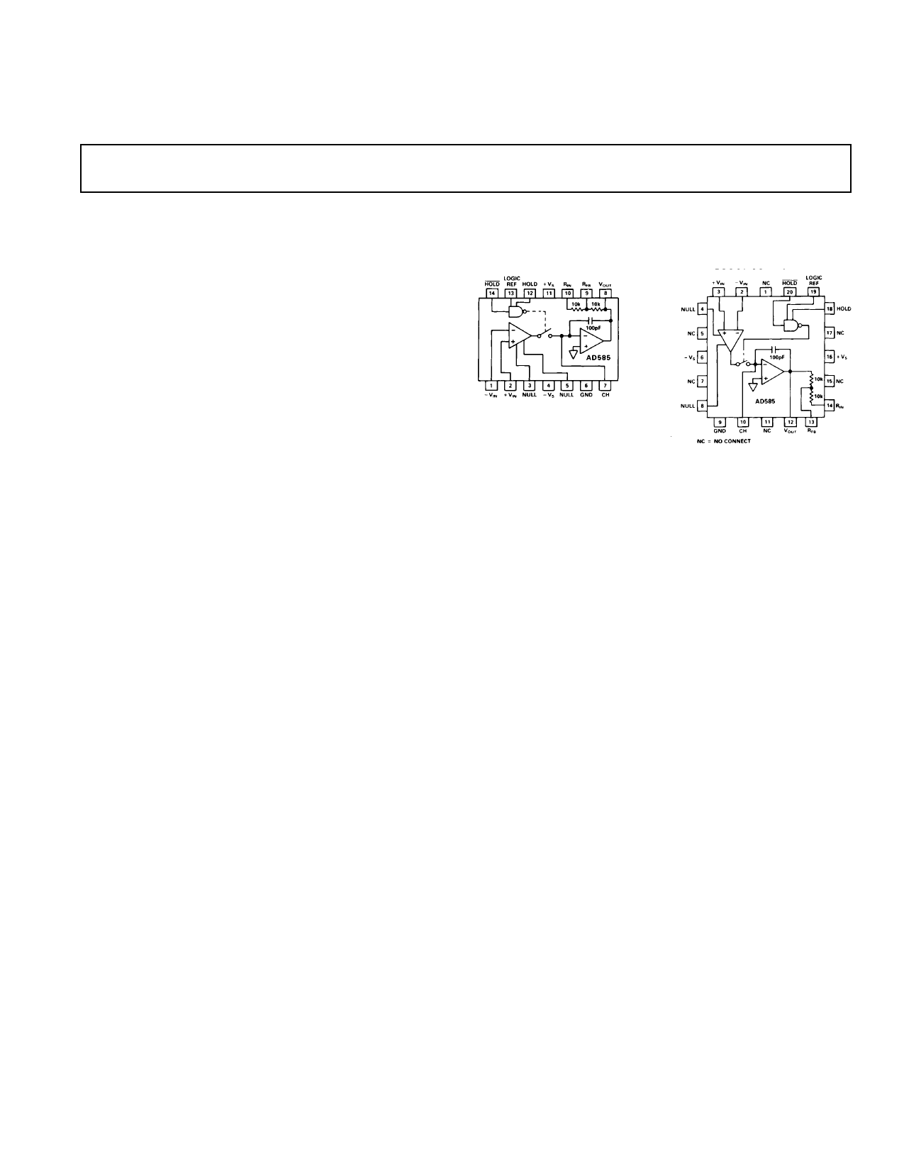
FUNCTIONAL BLOCK DIAGRAM
DIP LCC/PLCC Package
The AD585 is available in three performance grades. The JP
grade is specified for the 0°C to +70°C commercial temperature
range and packaged in a 20-pin PLCC. The AQ grade is speci-
fied for the –25°C to +85°C industrial temperature range and is
packaged in a 14-pin cerdip. The SQ and SE grades are speci-
fied for the –55°C to +125°C military temperature range and
are packaged in a 14-pin cerdip and 20-pin LCC.
PRODUCT HIGHLIGHTS
1. The fast acquisition time (3 µs) and low aperture jitter
(0.5 ns) make it the first choice for very high speed data
acquisition systems.
2. The droop rate is only 1.0 mV/ms so that it may be used in
slower high accuracy systems without the loss of accuracy.
3. The low charge transfer of the analog switch keeps sample-to
hold offset below 3 mV with the on-chip 100 pF hold capaci-
tor, eliminating the trade-off between acquisition time and
S/H offset required with other SHAs.
4. The AD585 has internal pretrimmed application resistors for
applications versatility.
5. The AD585 is complete with an internal hold capacitor for
ease of use. Capacitance can be added externally to reduce
the droop rate when long hold times and high accuracy are
required.
6. The AD585 is recommended for use with 10- and 12-bit
successive-approximation A/D converters such as AD573,
AD574A, AD674A, AD7572 and AD7672.
7. The AD585 is available in versions compliant with MIL-STD-
883. Refer to the Analog Devices Military Products Databook
or current AD585/883B data sheet for detailed specifications.
REV. A
Information furnished by Analog Devices is believed to be accurate and
reliable. However, no responsibility is assumed by Analog Devices for its
use, nor for any infringements of patents or other rights of third parties
which may result from its use. No license is granted by implication or
otherwise under any patent or patent rights of Analog Devices.
One Technology Way, P.O. Box 9106, Norwood, MA 02062-9106, U.S.A.
Tel: 617/329-4700
Fax: 617/326-8703
1 page 
AD585
For the AD585 in particular it becomes:
S/H
Offset
(V ) =
100
0.3 pC
pF + (CEXT
)
The addition of an external hold capacitor also affects the acqui-
sition time of the AD585. The change in acquisition time with
respect to the CEXT is shown graphically in Figure 2.
HOLD MODE
In the hold mode there are two important specifications that
must be considered; feedthrough and the droop rate. Feedthrough
errors appear as an attenuated version of the input at the output
while in the hold mode. Hold-Mode feedthrough varies with fre-
quency, increasing at higher frequencies. Feedthrough is an im-
portant specification when a sample and hold follows an analog
multiplexer that switches among many different channels.
Hold-mode droop rate is the change in output voltage per unit
of time while in the hold mode. Hold-mode droop originates as
leakage from the hold capacitor, of which the major leakage
current contributors are switch leakage current and bias current.
The rate of voltage change on the capacitor dV/dT is the ratio of
the total leakage current IL to the hold capacitance CH.
Droop
Rate
=
dVOUT
dT
(Volts/Sec) =
IL ( pA)
CH ( pF )
For the AD585 in particular;
Droop
Rate
=
100
100 pA
pF + (CEXT
)
Additionally the leakage current doubles for every 10°C increase
in temperature above 25°C; therefore, the hold-mode droop rate
characteristic will also double in the same fashion. The hold-mode
droop rate can be traded-off with acquisition time to provide the
best combination of droop error and acquisition time. The tradeoff
is easily accomplished by varying the value of CEXT.
Since a sample and hold is used typically in combination with
an A/D converter, then the total droop in the output voltage has
to be less than 1/2 LSB during the period of a conversion. The
maximum allowable signal change on the input of an A/D
converter is:
∆V max =
Full -Scale Voltage
2(N +1)
Once the maximum ∆V is determined then the conversion time
of the A/D converter (TCONV) is required to calculate the maxi-
mum allowable dV/dT.
dV
dt
max
=
∆V max
T CONV
dV max
The maximum dT as shown by the previous equation is
the limit not only at 25°C but at the maximum expected operat-
ing temperature range. Therefore, over the operating temperature
range the following criteria must be met (TOPERATION –25°C)
= ∆T.
(∆T °C)
dV 25° C × 2 10°C ≤ dV max
dT dT
HOLD-TO-SAMPLE TRANSITION
The Nyquist theorem states that a band-limited signal which is
sampled at a rate at least twice the maximum signal frequency
can be reconstructed without loss of information. This means
that a sampled data system must sample, convert and acquire
the next point at a rate at least twice the signal frequency. Thus
the maximum input frequency is equal to
( )f MAX =
1
2 T ACQ + TCONV + T AP
Where TACQ is the acquisition time of the sample-to-hold
amplifier, TAP is the maximum aperture time (small enough to
be ignored) and TCONV is the conversion time of the A/D
converter.
DATA ACQUISITION SYSTEMS
The fast acquisition time of the AD585 when used with a high
speed A/D converter allows accurate digitization of high fre-
quency signals and high throughput rates in multichannel data
acquisition systems. The AD585 can be used with a number of
different A/D converters to achieve high throughput rates. Fig-
ures 12 and 13 show the use of an AD585 with the AD578 and
AD574A.
Figure 12. A/D Conversion System, 117.6 kHz Throughput
58.8 kHz max Signal Input
Figure 13. 12-Bit A/D Conversion System, 26.3 kHz
Throughput Rate, 13.1 kHz max Signal Input
REV. A
–5–
5 Page | ||
| Páginas | Total 6 Páginas | |
| PDF Descargar | [ Datasheet AD585.PDF ] | |
Hoja de datos destacado
| Número de pieza | Descripción | Fabricantes |
| AD580 | High Precision 2.5 V IC Reference | Analog Devices |
| AD581 | High Precision 10 V IC Reference | Analog Devices |
| AD582 | Low Cost Sample/Hold Amplifier | Analog Devices |
| AD5821 | single 10-bit digital-to-analog converter | Analog Devices |
| Número de pieza | Descripción | Fabricantes |
| SLA6805M | High Voltage 3 phase Motor Driver IC. |
Sanken |
| SDC1742 | 12- and 14-Bit Hybrid Synchro / Resolver-to-Digital Converters. |
Analog Devices |
|
DataSheet.es es una pagina web que funciona como un repositorio de manuales o hoja de datos de muchos de los productos más populares, |
| DataSheet.es | 2020 | Privacy Policy | Contacto | Buscar |