|
|
|
PDF AD7878 Data sheet ( Hoja de datos )
| Número de pieza | AD7878 | |
| Descripción | LC2MOS Complete 12-Bit 100 kHz Sampling ADC with DSP Interface | |
| Fabricantes | Analog Devices | |
| Logotipo | ||
Hay una vista previa y un enlace de descarga de AD7878 (archivo pdf) en la parte inferior de esta página. Total 16 Páginas | ||
|
No Preview Available !
a LC2MOS Complete 12-Bit
100 kHz Sampling ADC with DSP Interface
AD7878
FEATURES
Complete ADC with DSP Interface, Comprising:
Track/Hold Amplifier with 2 s Acquisition Time
7 s A/D Converter
3 V Zener Reference
8-Word FIFO and Interface Logic
72 dB SNR at 10 kHz Input Frequency
Interfaces to High Speed DSP Processors, e.g.,
ADSP-2100, TMS32010, TMS32020
41 ns max Data Access Time
Low Power, 60 mW typ
APPLICATIONS
Digital Signal Processing
Speech Recognition and Synthesis
Spectrum Analysis
High Speed Modems
DSP Servo Control
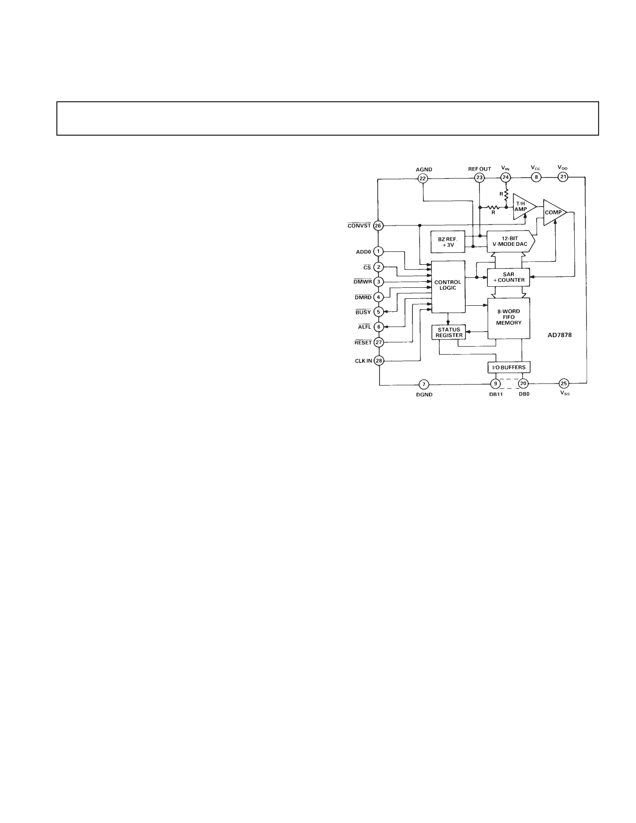
FUNCTIONAL BLOCK DIAGRAM
GENERAL DESCRIPTION
The AD7878 is a fast, complete, 12-bit A/D converter with a
versatile DSP interface consisting of an 8-word, first-in, first-out
(FIFO) memory and associated control logic.
The FIFO memory allows up to eight samples to be digitized
before the microprocessor is required to service the A/D con-
verter. The eight words can then be read out of the FIFO at
maximum microprocessor speed. A fast data access time of
41 ns allows direct interfacing to DSP processors and high
speed 16-bit microprocessors.
An on-chip status/control register allows the user to program the
effective length of the FIFO and contains the FIFO out of
range, FIFO empty and FIFO word count information.
The analog input of the AD7878 has a bipolar range of ± 3 V.
The AD7878 can convert full power signals up to 50 kHz and is
fully specified for dynamic parameters such as signal-to-noise
ratio and harmonic distortion.
The AD7878 is fabricated in Linear Compatible CMOS
(LC2MOS), an advanced, mixed technology process that com-
bines precision bipolar circuits with low power CMOS logic.
The part is available in four package styles, 28-pin plastic and
hermetic dual-in-line package (DIP), leadless ceramic chip
carrier (LCCC) or plastic leaded chip carrier (PLCC).
PRODUCT HIGHLIGHTS
1. Complete A/D Function with DSP Interface
The AD7878 provides the complete function for digitizing
ac signals to 12-bit accuracy. The part features an on-chip
track/hold, on-chip reference and 12-bit A/D converter. The
additional feature of an 8-word FIFO reduces the high soft-
ware overheads associated with servicing interrupts in DSP
processors.
2. Dynamic Specifications for DSP Users
The AD7878 is fully specified and tested for ac parameters,
including signal-to-noise ratio, harmonic distortion and
intermodulation distortion. Key digital timing parameters
are also tested and specified over the full operating tempera-
ture range.
3. Fast Microprocessor Interface
Data access time of 41 ns is the fastest ever achieved in a
monolithic A/D converter, and makes the AD7878 compat-
ible with all modern 16-bit microprocessors and digital
signal processors.
REV. A
Information furnished by Analog Devices is believed to be accurate and
reliable. However, no responsibility is assumed by Analog Devices for its
use, nor for any infringements of patents or other rights of third parties
which may result from its use. No license is granted by implication or
otherwise under any patent or patent rights of Analog Devices.
One Technology Way, P.O. Box 9106, Norwood, MA 02062-9106, U.S.A.
Tel: 617/329-4700
World Wide Web Site: http://www.analog.com
Fax: 617/326-8703
© Analog Devices, Inc., 1997
1 page 
AD7878
ORDERING GUIDE
Model1, 2
Temperature
Range
Signal-
to-Noise
Ratio
Data
Access
Time
Package
Options3
AD7878JN
AD7878AQ
AD7878SQ
AD7878KN
AD7878BQ
AD7878LN
AD7878SE4
AD7878JP
AD7878KP
AD7878LP
0°C to +70°C
–25°C to +85°C
–55°C to +125°C
0°C to +70°C
–25°C to +85°C
0°C to +70°C
–55°C to +125°C
0°C to +70°C
0°C to +70°C
0°C to +70°C
70 dB
70 dB
70 dB
72 dB
72 dB
72 dB
70 dB
70 dB
72 dB
72 dB
57 ns
57 ns
57 ns
57 ns
57 ns
41 ns
57 ns
57 ns
57 ns
41 ns
N-28
Q-28
Q-28
N-28
Q-28
N-28
E-28A
P-28A
P-28A
P-28A
NOTES
1To order MIL-STD-883, Class B processed parts, add /883B to part number.
Contact our local sales office for military data sheet.
2Analog Devices reserves the right to ship either ceramic (D-28) packages or
cerdip (Q-28) hermetic packages.
3E = Leadless Ceramic Chip Carrier; N = Plastic DIP; P = Plastic Leaded Chip
Carrier, Q = Cerdip.
4Available to /883B processing only.
STATUS/CONTROL REGISTER
The status/control register serves the dual function of providing
control and monitoring the status of the FIFO memory. This
register is directly accessible through the data bus (DB11–DB0)
with a read or write operation while ADD0 is high. A write
operation to the status/control register provides control for the
ALFL output, bus interface and FIFO counter reset. This is
normally done on power-up initialization. The FIFO memory
address pointer is incremented after each conversion and com-
pared with a preprogrammed count in the status/control regis-
ter. When this preprogrammed count is reached, the ALFL
output is asserted if the ENAF control bit is set to zero. This
ALFL can be used to interrupt the microprocessor after any
predetermined number of conversions (between 1 and 8). The
status of the address pointer along with sample overrange and
ALFL status can be accessed at any time by reading the status/
control register. Note: reading the status/control register does
not cause any internal data movement in the FIFO memory.
Status information for a particular word should be read from the
status register before the data word is read from the FIFO
memory.
STATUS/CONTROL REGISTER FUNCTION
DESCRIPTION
DB11 (ALFL)
Almost Full Flag, Read only. This is the same as Pin 6 (ALFL
output) status. A logic low indicates that the word count in
the FIFO memory has reached the preprogrammed count in bit
locations DB10–DB8. ALFL is updated at the end of conversion.
DB10–DB8 (AFC2–AFC0)
Almost Full Word Count, Read/Write. The count value deter-
mines the number of words in the FIFO memory, which will
cause ALFL to be set. When the FIFO word count equals the
programmed count in these three bits, both the ALFL output
and DB11 of the status register are set to a logic low. For ex-
ample, when a code of 011 is written to these bits, ALFL is set
when Location 0 through Location 3 of the FIFO memory
contains valid data. AFC2 is the most significant bit of the word
count. The count value can be read back if required.
DB7 (ENAF)
Enable Almost Full, Read/Write. Writing a 1 to this bit disables
the ALFL output and status register bit DB11.
DB6 (FOVR/RESET)
FIFO Overrun/RESET, Read/Write. Reading a 1 from this bit
indicates that at least one sample has been discarded because
the FIFO memory is full. When the FIFO is full (i.e., contains
eight words) any further conversion results will be lost. Writing
a 1 to this bit causes a system RESET as per the RESET input
(Pin 27).
DB5 (FOOR/DISO)
FIFO Out of RANGE/Disable Outputs, Read/Write. Reading a
1 from this bit indicates that at least one sample in the FIFO
memory is out of range. Writing a 0 to this bit prevents the data
bus from becoming active while BUSY is low, regardless of the
state of CS and DMRD.
DB4 (FEMP)
FIFO Empty, Read Only. Reading a 1 indicates there are no
samples in the FIFO memory. When the FIFO is empty the
internal ripple-down effects of the FIFO are disabled and fur-
ther reads will continue to access the last valid data word in
Location 0.
DB3 (SOOR)
Sample out of Range, Read Only. Reading a 1 indicates the next
sample to be read is out of range, i.e., the sample in Location 0
of the FIFO.
DB–DB0 (FCN2–FCN0)
FIFO Word Count, Read Only. The value read from these bits
indicates the number of samples in the FIFO memory. For
example, reading 011 from these bits indicates that Location 0
through Location 3 contains valid data. Note: reading all 0s
indicates there is either one word or no word in the FIFO
memory; in this case the FIFO Empty determines if there is no
word in memory. FCN2 is the most significant bit.
BIT LOCATION
STATUS INFORMATION (READ)
CONTROL FUNCTION (WRITE)
RESET STATUS
X =DON’T CARE
Table I. Status/Control Bit Function Description
DB11 DB10 DB9 DB8 DB7 DB6 DB5 DB4 DB3 DB2 DB1 DB0
ALFL
X
1
AFC2
AFC2
0
AFC1
AFC1
0
AFC0
AFC0
0
ENAF FOVR FOOR FEMP SOOR FCN2
ENAF RESET DISO X X X
000100
FCN1
X
0
FCN0
X
0
REV. A
–5–
5 Page 
Positive Full-Scale Adjust
Apply a voltage of 2.9978 V (FS/2 – 3/2 LSBs) at V1. Adjust R2
until the ADC output code flickers between 0111 1111 1110
and 0111 1111 1111.
Negative Full-Scale Adjust
Apply a voltage of –2.9993 V (–FS/2 + 1/2 LSB) at Vl and ad-
just R2 until the ADC output code flickers between 1000 0000
0000 and 1000 0000 0001.
AD7878
Figure 17. AD7878 Full-Scale Adjust Circuit
MICROPROCESSOR INTERFACING
The AD7878 high speed bus timing allows direct interfacing to
DSP processors. Due to the complexity of the AD7878 internal
logic, only synchronous interfacing is allowed. This means that
the ADC clock must be the same as, or a derivative of, the pro-
cessor clock. Suitable processor interfaces are shown in Figures
18 to 21.
AD7878–ADSP-2100/TMS32010/TMS32020
All three interfaces use an external timer for conversion control,
allowing the ADC to sample the analog input asynchronously to
the microprocessor. The AD7878 ALFL output interrupts the
processor when the FIFO preprogrammed word count is
reached. The processor then reads the conversion results from
the AD7878 internal FIFO memory.
Figure 19. AD7878–TMS32020 Interface
The interfaces to the ADSP-2100 and the TMS32020 gate the
AD7878 CS and the BUSY to provide a signal which drives the
processor into a wait state if a read/write operation to the ADC
is attempted while the ADC track/hold amplifier is going from
the track to the hold mode. This avoids digital feedthrough to
the analog circuitry. The TMS32020 does not have separate
RD and WR outputs to drive the AD7878 DMWR and
DMRD inputs. These are generated from the processor STRB
and R/W outputs with the addition of some logic gates.
Figure 18. AD7878–ADSP-2700 Interface
REV. A
Figure 20. AD7878–TMS32020 Interface
AD7878–M CC8000
This interface also uses an external timer for conversion control
as described for the previous three interfaces. It is discussed
separately because it needs extra logic due to the nature of its
interrupts. The MC68000 has eight levels of external interrupt.
When interrupting this processor one of these levels (0 to 7)
has to be encoded onto the IPL2–IPL0 inputs. This is achieved
with a 74148 encoder in Figure 21, (interrupt Level 1 is taken
for example purposes only). The MC68000 places this inter-
rupt level on address bits A3 to A1 at the start of the interrupt
service routine. Additional logic is used to decode this interrupt
level on the address bus and the FC2–FC0 outputs to generate
a VPA signal for the MC68000. This results in an autovectored
interrupt, the start address for the service routine must be
loaded into the appropriate auto vector location during initial-
ization. For further information on the 68000 interrupts con-
sult the 68000 User’s Manual.
–11–
11 Page | ||
| Páginas | Total 16 Páginas | |
| PDF Descargar | [ Datasheet AD7878.PDF ] | |
Hoja de datos destacado
| Número de pieza | Descripción | Fabricantes |
| AD7870 | LC2MOS Complete/ 12-Bit/ 100 kHz/ Sampling ADCs | Analog Devices |
| AD7870A | LC2MOS Complete/ 12-Bit/ 100 kHz / Sampling ADC | Analog Devices |
| AD7871 | LC2MOS Complete 14-Bit/ Sampling ADCs | Analog Devices |
| AD7872 | LC2MOS Complete 14-Bit/ Sampling ADCs | Analog Devices |
| Número de pieza | Descripción | Fabricantes |
| SLA6805M | High Voltage 3 phase Motor Driver IC. |
Sanken |
| SDC1742 | 12- and 14-Bit Hybrid Synchro / Resolver-to-Digital Converters. |
Analog Devices |
|
DataSheet.es es una pagina web que funciona como un repositorio de manuales o hoja de datos de muchos de los productos más populares, |
| DataSheet.es | 2020 | Privacy Policy | Contacto | Buscar |