|
|
|
PDF ADL5726 Data sheet ( Hoja de datos )
| Número de pieza | ADL5726 | |
| Descripción | Low Noise Amplifier | |
| Fabricantes | Analog Devices | |
| Logotipo | ||
Hay una vista previa y un enlace de descarga de ADL5726 (archivo pdf) en la parte inferior de esta página. Total 14 Páginas | ||
|
No Preview Available !
Data Sheet
21.2 GHz to 23.6 GHz, Low Noise Amplifier
ADL5726
FEATURES
Frequency range: 21.2 GHz to 23.6 GHz
Typical gain of >22.5 dB
Low noise input
Noise figure
3.3 dB typical at 21.2 GHz
3.4 dB typical at 23.6 GHz
High linearity input
≥1.0 dBm typical input third-order intercept (IIP3)
−8 dBm input 1 dB compression point (P1dB) at 23.6 GHz
Matched 50 Ω single-ended input
Matched 100 Ω differential outputs
8-lead, 2.00 mm × 2.00 mm LFCSP microwave packaging
APPLICATIONS
Point to point microwave radios
Instrumentation
Satellite communications (SATCOM)
Phased arrays
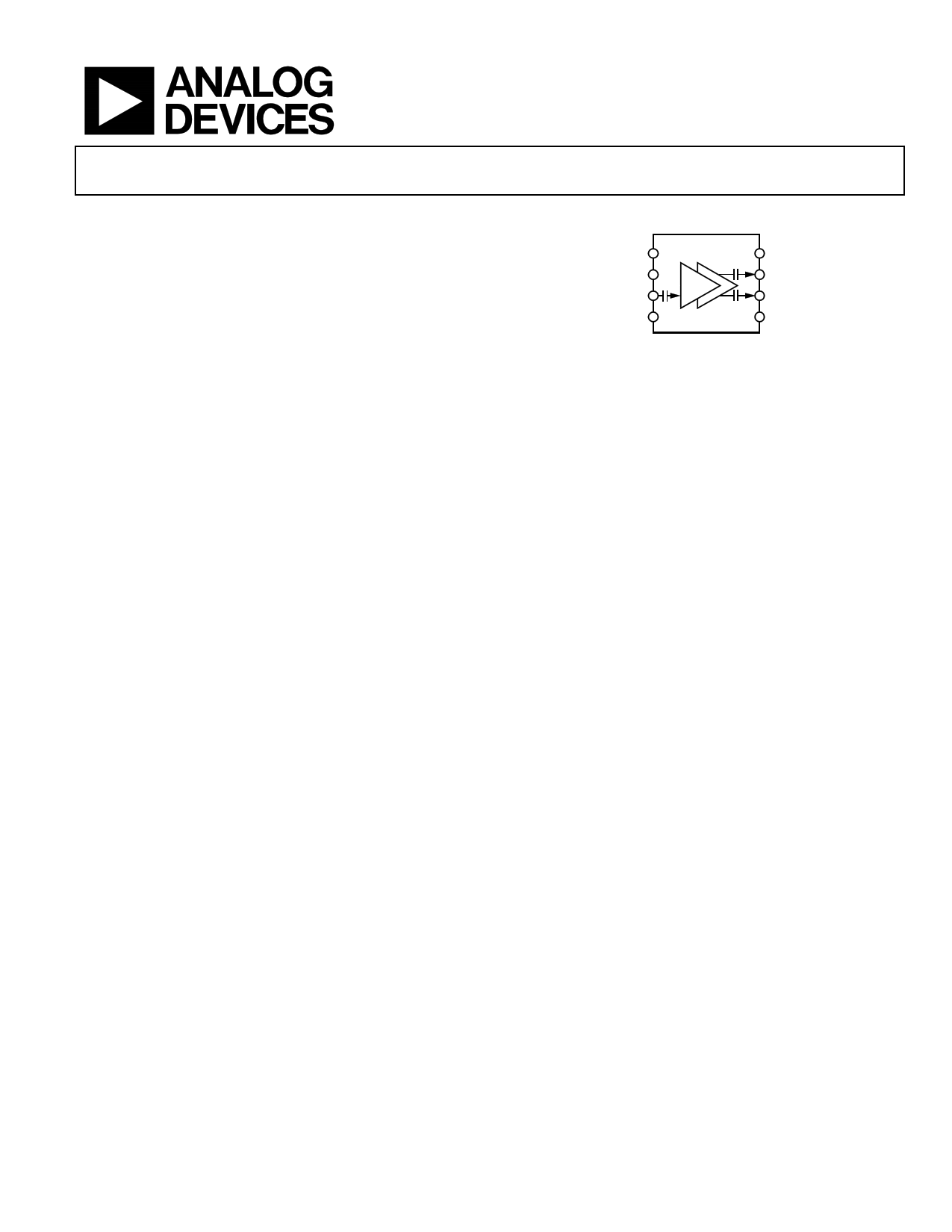
FUNCTIONAL BLOCK DIAGRAM
VCC1
ADL5726
VCC2
50Ω GND
SINGLE-ENDED
INPT
OUTN 100Ω
OUTP DIFFERENTIAL
RBIAS
DNC
DNC = DO NOT CONNECT.
DO NOT CONNECT TO THIS PIN.
Figure 1.
GENERAL DESCRIPTION
The ADL5726 is a narrow-band, high performance, low noise
amplifier (LNA) targeting microwave radio link receiver
designs. The monolithic silicon germanium (SiGe) design is
optimized for microwave radio link bands ranging from 21.2 GHz
to 23.6 GHz. The unique design offers a single-ended 50 Ω input
impedance and provides a 100 Ω balanced differential output
that is ideal for driving Analog Devices, Inc., differential
downconverters and radio frequency (RF) sampling analog-to-
digital converters (ADCs). This LNA provides noise figure
performance that, in the past, required more expensive three-
five (III-V) compounds process technology to achieve.
The ADL5721 and ADL5723 to ADL5726 family of narrow-
band LNAs are each packaged in a tiny, thermally enhanced,
2.00 mm × 2.00 mm LFCSP package. The ADL5721 and
ADL5723 to ADL5726 family operates over the temperature
range of −40°C to +85°C.
Rev. A
Document Feedback
Information furnished by Analog Devices is believed to be accurate and reliable. However, no
responsibility is assumed by Analog Devices for its use, nor for any infringements of patents or other
rights of third parties that may result from its use. Specifications subject to change without notice. No
license is granted by implication or otherwise under any patent or patent rights of Analog Devices.
Trademarksandregisteredtrademarksarethepropertyoftheirrespectiveowners.
One Technology Way, P.O. Box 9106, Norwood, MA 02062-9106, U.S.A.
Tel: 781.329.4700
©2016 Analog Devices, Inc. All rights reserved.
Technical Support
www.analog.com
1 page 
ADL5726
ABSOLUTE MAXIMUM RATINGS
Table 3.
Parameter
Supply Voltages
VCC1
VCC2
Maximum Junction Temperature
Operating Temperature Range
Storage Temperature Range
Lead Temperature Range (Soldering, 60 sec)
Rating
2.25 V
4.1 V
150°C/W
−40°C to +85°C
−55°C to +125°C
−65°C to +150°C
Stresses at or above those listed under Absolute Maximum
Ratings may cause permanent damage to the product. This is a
stress rating only; functional operation of the product at these
or any other conditions above those indicated in the operational
section of this specification is not implied. Operation beyond
the maximum operating conditions for extended periods may
affect product reliability.
Data Sheet
THERMAL RESISTANCE
θJA is thermal resistance, junction to ambient (°C/W), θJB is
thermal resistance, junction to board (°C/W), and θJC is thermal
resistance, junction to case (°C/W).
Table 4. Thermal Resistance
Package Type
θJA1 θJB1 θJC1 Unit
8-Lead LFCSP
39.90
23.88
3.71 °C/W
1 See JEDEC standard JESD51-2 for additional information on optimizing the
thermal impedance for a printed circuit board (PCB) with 3 × 4 vias.
ESD CAUTION
Rev. A | Page 4 of 13
5 Page 
ADL5726
PERFORMANCE UP TO 26.5 GHz
This section provides the test results at a higher frequency from
23.2 GHz to 26.5 GHz. Differential outputs are measured here.
Traces, hybrids, and connector losses were deembeded for all
measurements except output return loss. It is important to note
that this performance is typical and not guaranteed.
35
30
25
20
15
10
5
0
23.6
15
10
5
0
–5
–10
–15
–20
–25
23.6
15
10
5
0
–5
–10
–15
–20
–25
23.6
24.0 24.5 25.0 25.5
FREQUENCY (GHz)
Figure 18. Gain vs. Frequency
26.0
24.0 24.5 25.0 25.5 26.0
FREQUENCY (GHz)
Figure 19. Input P1dB vs. Frequency
24.0 24.5 25.0 25.5
FREQUENCY (GHz)
Figure 20. IIP3 vs. Frequency
26.0
26.5
26.5
26.5
Data Sheet
10
8
6
4
2
0
23.6 24.0 24.5 25.0 25.5 26.0 26.5
FREQUENCY (GHz)
Figure 21. Noise Figure vs. Frequency
0
–5
–10
–15
–20
–25
–30
23.6
0
24.0 24.5 25.0 25.5 26.0
FREQUENCY (GHz)
Figure 22. Input Return Loss vs. Frequency
26.5
–5
–10
–15
–20
–25
–30
23.6
24.0 24.5 25.0 25.5 26.0
FREQUENCY (GHz)
Figure 23. Output Return Loss vs. Frequency
26.5
Rev. A | Page 10 of 13
11 Page | ||
| Páginas | Total 14 Páginas | |
| PDF Descargar | [ Datasheet ADL5726.PDF ] | |
Hoja de datos destacado
| Número de pieza | Descripción | Fabricantes |
| ADL5721 | Low Noise Amplifier | Analog Devices |
| ADL5723 | Low Noise Amplifier | Analog Devices |
| ADL5724 | Low Noise Amplifier | Analog Devices |
| ADL5725 | Low Noise Amplifier | Analog Devices |
| Número de pieza | Descripción | Fabricantes |
| SLA6805M | High Voltage 3 phase Motor Driver IC. |
Sanken |
| SDC1742 | 12- and 14-Bit Hybrid Synchro / Resolver-to-Digital Converters. |
Analog Devices |
|
DataSheet.es es una pagina web que funciona como un repositorio de manuales o hoja de datos de muchos de los productos más populares, |
| DataSheet.es | 2020 | Privacy Policy | Contacto | Buscar |